Foreword
This document, started in early 1995, is considered the single most comprehensive technical reference to Game Boy available to the public.
You are reading a new version of it, maintained in the Markdown format and enjoying renewed community attention, correcting and updating it with recent findings. To learn more about the legacy and the mission of this initiative, check History.
SCOPE
The information here is targeted at homebrew development. Emulator developers may be also interested in the Game Boy: Complete Technical Reference document.
Contributing
This project is open source, released under the CC0 license. Everyone is welcome to help, provide feedback and propose additions or improvements. The git repository is hosted at github.com/gbdev/pandocs, where you can learn more about how you can contribute, find detailed contribution guidelines and procedures, file Issues and send Pull Requests.
There is a Discord chat dedicated to the gbdev community.
Finally, you can also contact us and send patches via email: pandocs (at) gbdev.io.
Using this document
In the top navigation bar, you will find a series of icons.
By clicking on the icon you will toggle an interactive table of contents to navigate the document. You can also use → and ← keys on your keyboard to go to the following and previous page.
The lets you choose among 5 different themes and color schemes to please your reading experience.
You can search anywhere by pressing s on your keyboard or clicking the icon.
The icon allows you to suggest an edit on the current page by directly opening the source file in the git repository.
This document version was produced from git commit a1703aa (2025-11-26 19:33:10 +0100).
Acknowledgements
The maintenance and expansion of this project wouldn’t be possible without the continued commitment and support of:
- The gbdev community, for providing precious feedback, content, support and invaluable knowledge.
- Contributors of code and content on the Pan Docs project.
- DigitalOcean, for sponsoring this initiative and lifting us from any hosting and infrastructural cost in the last few years.
- Backers, for allowing us to push the community projects further and spread open culture while staying independent and free.
Authors
Antonio Niño Díaz, Antonio Vivace, Beannaich, Cory Sandlin, Eldred “ISSOtm” Habert, Elizafox, Furrtek, Gekkio, Jeff Frohwein, John Harrison, Lior “LIJI32” Halphon, Mantidactyle, Marat Fayzullin, Martin “nocash” Korth, Pan of ATX, Pascal Felber, Paul Robson, T4g1, TechFalcon, endrift, exezin, jrra, kOOPa, mattcurrie, nitro2k01, pinobatch, Pat Fagan, Alvaro Burnett.
Special thanks
FrankenGraphics, zeta0134.
History
Pan Docs - also known as GAMEBOY.TXT or GBSPEC.TXT - is an old document dating back to early 1995, originally written by Pan of Anthrox. It has been one of the most important references for Game Boy hackers, emulators and homebrew developers during the last 25 years.
ADDRESS1.PCX, one of the diagrams attached to the first version, released January 28th, 1995
After its release (1995-2008), it received a number of revisions, corrections and updates, maintaining its TXT format. This folder provides a historical archive of those versions.
In 2008, a wikified version (using Martin Korth’s 2001 revision as a baseline) has been published. The document was split into different articles and it continued being maintained and updated in that form.
In 2020, after the discussion in this RFC we migrated the last updated version to plain Markdown and made github.com/gbdev/pandocs the new home of this resource, where it can receive new public discussions and contributions, maintain its legacy and historical relevance, while making use of modern tools and workflows to be visualized and distributed.
From 2020 to May 2021 we used VuePress to render the markdown files as web pages.
Since May 2021, we rely on mdBook.
We are releasing everything (content, sources, code, figures) under the CC0 license (Public Domain).
Specifications
| Game Boy (DMG) | Game Boy Pocket (MGB) | Super Game Boy (SGB) | Game Boy Color (CGB) | |
|---|---|---|---|---|
| CPU | 8-bit 8080-like Sharp CPU (speculated to be a SM83 core) | |||
| Master Clock | 4.194304 MHz1 | Depends on revision2 | Up to 8.388608 MHz | |
| System Clock | 1/4 the frequency of Master Clock | |||
| Work RAM | 8 KiB | 32 KiB3 (4 + 7 × 4 KiB) | ||
| Video RAM | 8 KiB | 16 KiB3 (2 × 8 KiB) | ||
| Screen | LCD 4.7 × 4.3 cm | LCD 4.8 × 4.4 cm | CRT TV | TFT 4.4 × 4 cm |
| Resolution | 160 × 144 | 160 × 144 within 256 × 224 border | 160 × 144 | |
| OBJ ("sprites") | 8 × 8 or 8 × 16 ; max 40 per screen, 10 per line | |||
| Palettes | BG: 1 × 4, OBJ: 2 × 3 | BG/OBJ: 1 + 4 × 3, border: 4 × 15 | BG: 8 × 4, OBJ: 8 × 33 | |
| Colors | 4 shades of green | 4 shades of gray | 32768 colors (15-bit RGB) | |
| Horizontal sync | 9.198 KHz | Complicated4 | 9.198 KHz | |
| Vertical sync | 59.73 Hz | Complicated4 | 59.73 Hz | |
| Sound | 4 channels with stereo output | 4 GB channels + SNES audio | 4 channels with stereo output | |
| Power | DC 6V, 0.7 W | DC 3V, 0.7 W | Powered by SNES | DC 3V, 0.6 W |
Real DMG units tend to run about 50-70 PPM slow. Accuracy of other models is unknown. See this page for more details.
SGB1 cartridges derive the GB CPU clock from the SNES’ clock, yielding a clock speed a bit higher, which differs slightly between NTSC and PAL systems. SGB2 instead uses a clock internal to the cartridge, and so has the same speed as the handhelds.
The same value as on DMG is used in compatibility mode.
The SGB runs two consoles: a Game Boy within the SGB cartridge, and the SNES itself. The GB LCD output is captured and displayed by the SNES, but the two consoles’ frame rates don’t quite sync up, leading to duplicated and/or dropped frames. The GB side of the vertical sync depends on the CPU clock2, with the same ratio as the handhelds.
Memory Map
The Game Boy has a 16-bit address bus, which is used to address ROM, RAM, and I/O.
| Start | End | Description | Notes |
|---|---|---|---|
| 0000 | 3FFF | 16 KiB ROM bank 00 | From cartridge, usually a fixed bank |
| 4000 | 7FFF | 16 KiB ROM Bank 01–NN | From cartridge, switchable bank via mapper (if any) |
| 8000 | 9FFF | 8 KiB Video RAM (VRAM) | In CGB mode, switchable bank 0/1 |
| A000 | BFFF | 8 KiB External RAM | From cartridge, switchable bank if any |
| C000 | CFFF | 4 KiB Work RAM (WRAM) | |
| D000 | DFFF | 4 KiB Work RAM (WRAM) | In CGB mode, switchable bank 1–7 |
| E000 | FDFF | Echo RAM (mirror of C000–DDFF) | Nintendo says use of this area is prohibited. |
| FE00 | FE9F | Object attribute memory (OAM) | |
| FEA0 | FEFF | Not Usable | Nintendo says use of this area is prohibited. |
| FF00 | FF7F | I/O Registers | |
| FF80 | FFFE | High RAM (HRAM) | |
| FFFF | FFFF | Interrupt Enable register (IE) |
I/O Ranges
The Game Boy uses the following I/O ranges:
| Start | End | First appeared | Purpose |
|---|---|---|---|
| $FF00 | DMG | Joypad input | |
| $FF01 | $FF02 | DMG | Serial transfer |
| $FF04 | $FF07 | DMG | Timer and divider |
| $FF0F | DMG | Interrupts | |
| $FF10 | $FF26 | DMG | Audio |
| $FF30 | $FF3F | DMG | Wave pattern |
| $FF40 | $FF4B | DMG | LCD Control, Status, Position, Scrolling, and Palettes |
| $FF46 | DMG | OAM DMA transfer | |
| $FF4C | $FF4D | CGB | KEY0 and KEY1 |
| $FF4F | CGB | VRAM Bank Select | |
| $FF50 | DMG | Boot ROM mapping control | |
| $FF51 | $FF55 | CGB | VRAM DMA |
| $FF56 | CGB | IR port | |
| $FF68 | $FF6B | CGB | BG / OBJ Palettes |
| $FF6C | CGB | Object priority mode | |
| $FF70 | CGB | WRAM Bank Select |
VRAM memory map
VRAM is, by itself, normal RAM, and may be used as such; however, the PPU interprets it in specific ways.
Bank 1 does not exist except on CGB, where it can be switched to (only in CGB Mode) using the VBK register.
Each bank first contains 384 tiles, of 16 bytes each. These tiles are commonly thought of as grouped in three “blocks” of 128 tiles each; see this detailed explanation for more details.
The ID of a tile can be obtained from its address using the following equation:
ID = address / 16 mod 256.
This is equivalent to only looking at the address’ middle two hexadecimal digits.
After the tiles, each bank contains two maps, 32×32 (= 1024) bytes each. The two banks are however different here: bank 0 contains tile maps, while bank 1 contains the corresponding attribute maps.
Each entry corresponds to a set of coordinates, linked to its address:
- X = address mod 32
- Y = address / 32 mod 32
In fact, the address of any entry can be thought of as a bitfield:
| 15 | 14 | 13 | 12 | 11 | 10 | 9 | 8 | 7 | 6 | 5 | 4 | 3 | 2 | 1 | 0 |
|---|---|---|---|---|---|---|---|---|---|---|---|---|---|---|---|
| 1 | 0 | 0 | 1 | 1 | tilemap | Y | X | ||||||||
Here is a visualisation of how VRAM is laid out; hover over elements to see some details.
The diagram is not to scale: each map takes up only half as much memory as a tile "block", despite the maps being visually twice as tall.Jump Vectors in first ROM bank
The following addresses are supposed to be used as jump vectors:
- RST instructions: 0000, 0008, 0010, 0018, 0020, 0028, 0030, 0038
- Interrupts: 0040, 0048, 0050, 0058, 0060
However, this memory area (0000-00FF) may be used for any other purpose in case that your
program doesn’t use any (or only some) rst instructions or interrupts. rst
is a 1-byte instruction that works similarly to the 3-byte call instruction, except
that the destination address is restricted. Since it is 1-byte sized,
it is also slightly faster.
Cartridge Header in first ROM bank
The memory area at 0100-014F contains the cartridge header. This area contains information about the program, its entry point, checksums, information about the used MBC chip, the ROM and RAM sizes, etc. Most of the bytes in this area are required to be specified correctly.
External Memory and Hardware
The areas from 0000-7FFF and A000-BFFF address external hardware on the cartridge, which is essentially an expansion board. Typically this is a ROM and SRAM or, more often, a Memory Bank Controller (MBC). The RAM area can be read from and written to normally; writes to the ROM area control the MBC. Some MBCs allow mapping of other hardware into the RAM area in this way.
Cartridge RAM is often battery buffered to hold saved game positions, high score tables, and other information when the Game Boy is turned off. For specific information read the chapter about Memory Bank Controllers.
Echo RAM
The range E000-FDFF is mapped to WRAM, but only the lower 13 bits of the address lines are connected, with the upper bits on the upper bank set internally in the memory controller by a bank swap register. This causes the address to effectively wrap around. All reads and writes to this range have the same effect as reads and writes to C000-DDFF.
Nintendo prohibits developers from using this memory range. The behavior is confirmed on all official hardware. Some emulators (such as VisualBoyAdvance <1.8) don’t emulate Echo RAM. In some flash cartridges, echo RAM interferes with SRAM normally at A000-BFFF. Software can check if Echo RAM is properly emulated by writing to RAM (avoid values 00 and FF) and checking if said value is mirrored in Echo RAM and not cart SRAM.
FEA0–FEFF range
Nintendo indicates use of this area is prohibited. This area returns $FF when OAM is blocked, and otherwise the behavior depends on the hardware revision.
-
On DMG, MGB, SGB, and SGB2, reads during OAM block trigger OAM corruption. Reads otherwise return $00.
-
On CGB revisions 0-D, this area is a unique RAM area, but is masked with a revision-specific value.
-
On CGB revision E, AGB, AGS, and GBP, it returns the high nibble of the lower address byte twice, e.g. FFAx returns $AA, FFBx returns $BB, and so forth.
Hardware Registers
| Address | Name | Description | Readable / Writable | Models |
|---|---|---|---|---|
| $FF00 | P1/JOYP | Joypad | Mixed | All |
| $FF01 | SB | Serial transfer data | R/W | All |
| $FF02 | SC | Serial transfer control | R/W | Mixed |
| $FF04 | DIV | Divider register | R/W | All |
| $FF05 | TIMA | Timer counter | R/W | All |
| $FF06 | TMA | Timer modulo | R/W | All |
| $FF07 | TAC | Timer control | R/W | All |
| $FF0F | IF | Interrupt flag | R/W | All |
| $FF10 | NR10 | Sound channel 1 sweep | R/W | All |
| $FF11 | NR11 | Sound channel 1 length timer & duty cycle | Mixed | All |
| $FF12 | NR12 | Sound channel 1 volume & envelope | R/W | All |
| $FF13 | NR13 | Sound channel 1 period low | W | All |
| $FF14 | NR14 | Sound channel 1 period high & control | Mixed | All |
| $FF16 | NR21 | Sound channel 2 length timer & duty cycle | Mixed | All |
| $FF17 | NR22 | Sound channel 2 volume & envelope | R/W | All |
| $FF18 | NR23 | Sound channel 2 period low | W | All |
| $FF19 | NR24 | Sound channel 2 period high & control | Mixed | All |
| $FF1A | NR30 | Sound channel 3 DAC enable | R/W | All |
| $FF1B | NR31 | Sound channel 3 length timer | W | All |
| $FF1C | NR32 | Sound channel 3 output level | R/W | All |
| $FF1D | NR33 | Sound channel 3 period low | W | All |
| $FF1E | NR34 | Sound channel 3 period high & control | Mixed | All |
| $FF20 | NR41 | Sound channel 4 length timer | W | All |
| $FF21 | NR42 | Sound channel 4 volume & envelope | R/W | All |
| $FF22 | NR43 | Sound channel 4 frequency & randomness | R/W | All |
| $FF23 | NR44 | Sound channel 4 control | Mixed | All |
| $FF24 | NR50 | Master volume & VIN panning | R/W | All |
| $FF25 | NR51 | Sound panning | R/W | All |
| $FF26 | NR52 | Sound on/off | Mixed | All |
| $FF30-FF3F | Wave RAM | Storage for one of the sound channels’ waveform | R/W | All |
| $FF40 | LCDC | LCD control | R/W | All |
| $FF41 | STAT | LCD status | Mixed | All |
| $FF42 | SCY | Viewport Y position | R/W | All |
| $FF43 | SCX | Viewport X position | R/W | All |
| $FF44 | LY | LCD Y coordinate | R | All |
| $FF45 | LYC | LY compare | R/W | All |
| $FF46 | DMA | OAM DMA source address & start | R/W | All |
| $FF47 | BGP | BG palette data | R/W | DMG |
| $FF48 | OBP0 | OBJ palette 0 data | R/W | DMG |
| $FF49 | OBP1 | OBJ palette 1 data | R/W | DMG |
| $FF4A | WY | Window Y position | R/W | All |
| $FF4B | WX | Window X position plus 7 | R/W | All |
| $FF4C | KEY0/SYS | CPU mode select | Mixed | CGB |
| $FF4D | KEY1/SPD | Prepare speed switch | Mixed | CGB |
| $FF4F | VBK | VRAM bank | R/W | CGB |
| $FF50 | BANK | Boot ROM mapping control | W | All |
| $FF51 | HDMA1 | VRAM DMA source high | W | CGB |
| $FF52 | HDMA2 | VRAM DMA source low | W | CGB |
| $FF53 | HDMA3 | VRAM DMA destination high | W | CGB |
| $FF54 | HDMA4 | VRAM DMA destination low | W | CGB |
| $FF55 | HDMA5 | VRAM DMA length/mode/start | R/W | CGB |
| $FF56 | RP | Infrared communications port | Mixed | CGB |
| $FF68 | BCPS/BGPI | Background color palette specification / Background palette index | R/W | CGB |
| $FF69 | BCPD/BGPD | Background color palette data / Background palette data | R/W | CGB |
| $FF6A | OCPS/OBPI | OBJ color palette specification / OBJ palette index | R/W | CGB |
| $FF6B | OCPD/OBPD | OBJ color palette data / OBJ palette data | R/W | CGB |
| $FF6C | OPRI | Object priority mode | R/W | CGB |
| $FF70 | SVBK/WBK | WRAM bank | R/W | CGB |
| $FF76 | PCM12 | Audio digital outputs 1 & 2 | R | CGB |
| $FF77 | PCM34 | Audio digital outputs 3 & 4 | R | CGB |
| $FFFF | IE | Interrupt enable | R/W | All |
Graphics Overview
The Game Boy outputs graphics to a 160×144 pixel LCD, using a quite complex mechanism to facilitate rendering.
Terminology
Sprites/graphics terminology can vary a lot among different platforms, consoles, users and communities. You may be familiar with slightly different definitions. Keep also in mind that some definitions refer to lower (hardware) tools and some others to higher abstractions concepts.
Tiles
Similarly to other retro systems, pixels are not manipulated individually, as this would be expensive CPU-wise. Instead, pixels are grouped in 8×8 squares, called tiles (or sometimes “patterns” or “characters”), often considered as the base unit in Game Boy graphics.
A tile does not encode color information. Instead, a tile assigns a color indices to each of its pixels, ranging from 0 to 3. For this reason, Game Boy graphics are also called 2bpp (2 bits per pixel). When a tile is used in the Background or Window, these color indices are associated with a palette. When a tile is used in an object, the indices 1 to 3 are associated with a palette, but ID 0 means transparent.
Palettes
A palette consists of an array of colors, 4 in the Game Boy’s case. Palettes are stored differently in monochrome and color versions of the console.
Modifying palettes enables graphical effects such as quickly flashing some graphics (damage, invulnerability, thunderstorm, etc.), fading the screen, “palette swaps”, and more.
Layers
The Game Boy has three “layers”, from back to front: the Background, the Window, and the Objects. Some features and behaviors break this abstraction, but it works for the most part.
Background
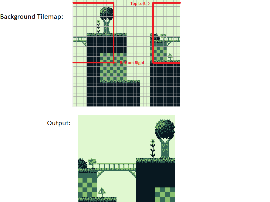
The background is composed of a tilemap. A tilemap is a large grid of tiles. However, tiles aren’t directly written to tilemaps, they merely contain references to the tiles. This makes reusing tiles very cheap, both in CPU time and in required memory space, and it is the main mechanism that helps work around the paltry 8 KiB of video RAM.
The background can be made to scroll as a whole, writing to two hardware registers. This makes scrolling very cheap.
Window
The window is sort of a second background layer on top of the background. It is fairly limited: it has no transparency, it’s always a rectangle and only the position of the top-left pixel can be controlled.
Possible usage include a fixed status bar in an otherwise scrolling game (e.g. Super Mario Land 2).
Objects
The background layer is useful for elements scrolling as a whole, but it’s impractical for objects that need to move separately, such as the player.
The objects layer is designed to fill this gap: objects are made of 1 or 2 stacked tiles (8×8 or 8×16 pixels) and can be displayed anywhere on the screen.
NOTE
Several objects can be combined (they can be called metasprites) to draw a larger graphical element, usually called “sprite”. Originally, the term “sprites” referred to fixed-sized objects composited together, by hardware, with a background. Use of the term has since become more general.
To summarise:
- Tile, an 8×8-pixel chunk of graphics.
- Object, an entry in object attribute memory, composed of 1 or 2 tiles. Can be moved independently of the background.
VRAM Tile Data
Tile data is stored in VRAM in the memory area at $8000-$97FF; with each tile taking 16 bytes, this area defines data for 384 tiles. In CGB Mode, this is doubled (768 tiles) because of the two VRAM banks.
Each tile (or character) has 8×8 pixels and has a color depth of 2 bits per pixel, allowing each pixel to use one of 4 colors or gray shades. Tiles can be displayed as part of the Background/Window maps, and/or as objects (movable sprites). Color 0 has a special meaning in objects - it’s transparent, allowing the background or other objects behind it to show through.
There are three “blocks” of 128 tiles each:
| Tile IDs for... | Block 0 | Block 1 | Block 2 |
|---|---|---|---|
| $8000–87FF | $8800–8FFF | $9000–97FF | |
| Objects | 0–127 | 128–255 | — |
| BG/Win, if LCDC.4=1 | 0–127 | 128–255 | — |
| BG/Win, if LCDC.4=0 | — | 128–255 | 0–127 |
Tiles are always indexed using an 8-bit integer, but the addressing method may differ:
- The “$8000 method” uses $8000 as its base pointer and uses an unsigned addressing, meaning that tiles 0-127 are in block 0, and tiles 128-255 are in block 1.
- The “$8800 method” uses $9000 as its base pointer and uses a signed addressing, meaning that tiles 0-127 are in block 2, and tiles -128 to -1 are in block 1; or, to put it differently, “$8800 addressing” takes tiles 0-127 from block 2 and tiles 128-255 from block 1.
(You can notice that block 1 is shared by both addressing methods)
Objects always use “$8000 addressing”, but the BG and Window can use either mode, controlled by LCDC bit 4.
Data format
Each tile occupies 16 bytes, where each line is represented by 2 bytes:
| Byte | 1st | 2nd | 3rd | 4th | ... |
|---|---|---|---|---|---|
| Explanation | Topmost line (top 8 pixels) | Second line | Etc. | ||
For each line, the first byte specifies the least significant bit of the color
ID of each pixel, and the second byte specifies the most significant bit. In
both bytes, bit 7 represents the leftmost pixel, and bit 0 the rightmost. For
example, the tile data $3C $7E $42 $42 $42 $42 $42 $42 $7E $5E $7E $0A $7C $56 $38 $7C appears as follows:
For the first row, the values $3C $7E are 00111100 and 01111110 in
binary. The leftmost bits are 0 and 0, thus the color index is binary 00, or 0.
The next bits are 0 and 1, thus the color index is binary 10, or 2 (remember to
flip the order of the bits!). The full eight-pixel row evaluates to 0 2 3 3 3 3
2 0.
A tool for viewing tiles can be found here.
So, each pixel has a color index of 0 to 3. The color numbers are translated into real colors (or gray shades) depending on the current palettes, except that when the tile is used in an OBJ the color index 0 means transparent. The palettes are defined through registers BGP, OBP0 and OBP1, and BCPS/BGPI, BCPD/BGPD, OCPS/OBPI and OCPD/OBPD (CGB Mode).
VRAM Tile Maps
The Game Boy contains two 32×32 tile maps in VRAM at
the memory areas $9800-$9BFF and $9C00-$9FFF. Any of these maps can be used to
display the Background or the Window.
Tile Indexes
Each tile map contains the 1-byte indexes of the tiles to be displayed.
Tiles are obtained from the Tile Data Table using either of the two addressing modes (described in VRAM Tile Data), which can be selected via the LCDC register.
Since one tile has 8×8 pixels, each map holds a 256×256 pixels picture. Only 160×144 of those pixels are displayed on the LCD at any given time.
BG Map Attributes (CGB Mode only)
In CGB Mode, an additional map of 32×32 bytes is stored in VRAM Bank 1 (each byte defines attributes for the corresponding tile-number map entry in VRAM Bank 0, that is, 1:9800 defines the attributes for the tile at 0:9800):
| 7 | 6 | 5 | 4 | 3 | 2 | 1 | 0 | |
|---|---|---|---|---|---|---|---|---|
| BG attributes | Priority | Y flip | X flip | Bank | Color palette | |||
- Priority:
0= No;1= Color indices 1–3 of the corresponding BG/Window tile are drawn over OBJ, regardless of OBJ priority - Y flip:
0= Normal;1= Tile is drawn vertically mirrored - X flip:
0= Normal;1= Tile is drawn horizontally mirrored - Bank:
0= Fetch tile from VRAM bank 0;1= Fetch tile from VRAM bank 1 - Color palette: Which of BGP0–7 to use
Bit 4 is ignored by the hardware, but can be written to and read from normally.
Note that, for example, if the byte at 0:9800 is $2A, the attribute at 1:9800 doesn’t define properties for ALL tiles $2A on-screen, but only the one at 0:9800!
BG-to-OBJ Priority in CGB Mode
In CGB Mode, the priority between the BG (and window) layer and the OBJ layer is declared in three different places:
We can infer the following rules from the table below:
- If the BG color index is 0, the OBJ will always have priority;
- Otherwise, if LCDC bit 0 is clear, the OBJ will always have priority;
- Otherwise, if both the BG Attributes and the OAM Attributes have bit 7 clear, the OBJ will have priority;
- Otherwise, BG will have priority.
The following table shows the relations between the 3 flags:
| LCDC bit 0 | OAM attr bit 7 | BG attr bit 7 | Priority |
|---|---|---|---|
| 0 | 0 | 0 | OBJ |
| 0 | 0 | 1 | OBJ |
| 0 | 1 | 0 | OBJ |
| 0 | 1 | 1 | OBJ |
| 1 | 0 | 0 | OBJ |
| 1 | 0 | 1 | BG color 1–3, otherwise OBJ |
| 1 | 1 | 0 | BG color 1–3, otherwise OBJ |
| 1 | 1 | 1 | BG color 1–3, otherwise OBJ |
This test ROM can be used to observe the above.
Keep in mind that:
- OAM Attributes bit 7 will grant OBJ priority when clear, not when set.
- Priority between all OBJs is resolved before priority with the BG layer is considered. Please refer to this page for more details.
Background (BG)
The SCY and SCX registers can be used to scroll the Background, specifying the origin of the visible 160×144 pixel area within the total 256×256 pixel Background map. The visible area of the Background wraps around the Background map (that is, when part of the visible area goes beyond the map edge, it starts displaying the opposite side of the map).
In Non-CGB mode, the Background (and the Window) can be disabled using LCDC bit 0.
Window
Besides the Background, there is also a Window overlaying it. The content of the Window is not scrollable; it is always displayed starting at the top left tile of its tile map. The only way to adjust the Window is by modifying its position on the screen, which is done via the WX and WY registers. The screen coordinates of the top left corner of the Window are (WX-7,WY). The tiles for the Window are stored in the Tile Data Table. Both the Background and the Window share the same Tile Data Table.
Whether the Window is displayed can be toggled using LCDC bit 5. But in Non-CGB mode this bit is only functional as long as LCDC bit 0 is set. Enabling the Window makes Mode 3 slightly longer on scanlines where it’s visible. (See WX and WY for the definition of “Window visibility”.)
Window Internal Line Counter
The window keeps an internal line counter that’s functionally similar to LY, and increments alongside it. However, it only gets incremented when the window is visible, as described here.
This line counter determines what window line is to be rendered on the current scanline.
Object Attribute Memory (OAM)
The Game Boy PPU can display up to 40 movable objects (or sprites), each 8×8 or 8×16 pixels. Because of a limitation of hardware, only ten objects can be displayed per scanline. Object tiles have the same format as BG tiles, but they are taken from tile blocks 0 and 1 located at $8000-8FFF and have unsigned numbering.
Object attributes reside in the object attribute memory (OAM) at $FE00-FE9F. (This corresponds to the sprite attribute table on a TMS9918 VDP.) Each of the 40 entries consists of four bytes with the following meanings:
Byte 0 — Y Position
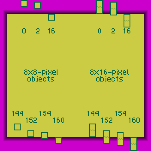
Y = Object’s vertical position on the screen + 16. So for example:
- Y=0 hides an object,
- Y=2 hides an 8×8 object but displays the last two rows of an 8×16 object,
- Y=16 displays an object at the top of the screen,
- Y=144 displays an 8×16 object aligned with the bottom of the screen,
- Y=152 displays an 8×8 object aligned with the bottom of the screen,
- Y=154 displays the first six rows of an object at the bottom of the screen,
- Y=160 hides an object.
Byte 1 — X Position
X = Object’s horizontal position on the screen + 8. This works similarly to the examples above, except that the width of an object is always 8. An off-screen value (X=0 or X>=168) hides the object, but the object still contributes to the limit of ten objects per scanline. This can cause objects later in OAM not to be drawn on that line. A better way to hide an object is to set its Y-coordinate off-screen.
Byte 2 — Tile Index
In 8×8 mode (LCDC bit 2 = 0), this byte specifies the object’s only tile index ($00-$FF). This unsigned value selects a tile from the memory area at $8000-$8FFF. In CGB Mode this could be either in VRAM bank 0 or 1, depending on bit 3 of the following byte. In 8×16 mode (LCDC bit 2 = 1), the memory area at $8000-$8FFF is still interpreted as a series of 8×8 tiles, where every 2 tiles form an object. In this mode, this byte specifies the index of the first (top) tile of the object. This is enforced by the hardware: the least significant bit of the tile index is ignored; that is, the top 8×8 tile is “NN & $FE”, and the bottom 8×8 tile is “NN | $01”.
Byte 3 — Attributes/Flags
| 7 | 6 | 5 | 4 | 3 | 2 | 1 | 0 | |
|---|---|---|---|---|---|---|---|---|
| Attributes | Priority | Y flip | X flip | DMG palette | Bank | CGB palette | ||
- Priority:
0= No,1= BG and Window color indices 1–3 are drawn over this OBJ - Y flip:
0= Normal,1= Entire OBJ is vertically mirrored - X flip:
0= Normal,1= Entire OBJ is horizontally mirrored - DMG palette [Non CGB Mode only]:
0= OBP0,1= OBP1 - Bank [CGB Mode Only]:
0= Fetch tile from VRAM bank 0,1= Fetch tile from VRAM bank 1 - CGB palette [CGB Mode Only]: Which of OBP0–7 to use
Writing data to OAM
The recommended method is to write the data to a buffer in normal RAM (typically WRAM) first, then to copy that buffer to OAM using the DMA transfer functionality.
While it is also possible to write data directly to the OAM area by accessing it normally, this only works during the HBlank and VBlank periods.
Object Priority and Conflicts
There are two kinds of “priorities” as far as objects are concerned. The first one defines which objects are ignored when there are more than 10 on a given scanline. The second one decides which object is displayed on top when some overlap (the Game Boy being a 2D console, there is no Z coordinate).
Selection priority
During each scanline’s OAM scan, the PPU compares LY
(using LCDC bit 2 to determine their size) to each
object’s Y position to select up to 10 objects to be drawn on that line.
The PPU scans OAM sequentially (from $FE00 to $FE9F), selecting the first (up to)
10 suitably-positioned objects.
Since the PPU only checks the Y coordinate to select objects, even off-screen objects count towards the 10-objects-per-scanline limit. Merely setting an object’s X coordinate to X = 0 or X ≥ 168 (160 + 8) will hide it, but it will still count towards the limit, possibly causing another object later in OAM not to be drawn. To keep off-screen objects from affecting on-screen ones, make sure to set their Y coordinate to Y = 0 or Y ≥ 160 (144 + 16). (Y ≤ 8 also works if object size is set to 8×8.)
Drawing priority
When opaque pixels from two different objects overlap, which pixel ends up being displayed is determined by another kind of priority: the pixel belonging to the higher-priority object wins. However, this priority is determined differently when in CGB mode.
- In Non-CGB mode, the smaller the X coordinate, the higher the priority. When X coordinates are identical, the object located first in OAM has higher priority.
- In CGB mode, only the object’s location in OAM determines its priority. The earlier the object, the higher its priority.
Interaction with "BG over OBJ" flag
Object drawing priority and “BG over OBJ” interact in a non-intuitive way.
Internally, the PPU first resolves priority between objects to pick an “object pixel”, which is the first non-transparent pixel encountered when iterating over objects sorted by their drawing priority. The “BG over OBJ” attribute is never considered in this process.
Only after object priority is resolved, the “object pixel” has the “BG over OBJ” attribute of its object checked to determine whether it should be drawn over the background. This means that an object with a higher priority but with “BG over OBJ” enabled will sort of “mask” lower-priority objects, even if those have “BG over OBJ” disabled.
This can be exploited to only hide parts of an object behind the background (video demonstration). A similar behaviour can be seen on the NES.
In CGB Mode, BG vs. OBJ priority is declared in more than one register, please see this page for more details.
OAM DMA Transfer
FF46 — DMA: OAM DMA source address & start
Writing to this register starts a DMA transfer from ROM or RAM to OAM (Object Attribute Memory). The written value specifies the transfer source address divided by $100, that is, source and destination are:
Source:      $XX00-$XX9F   ;XX = $00 to $DF
Destination: $FE00-$FE9F
The transfer takes 160 M-cycles: 640 dots (1.4 lines) in normal speed, or 320 dots (0.7 lines) in CGB Double Speed Mode. This is much faster than a CPU-driven copy.
OAM DMA bus conflicts
On DMG, during OAM DMA, the CPU can access only HRAM (memory at $FF80-$FFFE). For this reason, the programmer must copy a short procedure (see below) into HRAM, and use this procedure to start the transfer from inside HRAM, and wait until the transfer has finished.
On CGB, the cartridge and WRAM are on separate buses.
This means that the CPU can access ROM or cartridge SRAM during OAM DMA from WRAM, or WRAM during OAM DMA from ROM or SRAM.
However, because a call writes a return address to the stack, and the stack and variables are usually in WRAM,
it’s still recommended to busy-wait in HRAM for DMA to finish even on CGB.
Interrupts
An interrupt writes a return address to the stack and fetches the interrupt handler’s instructions from ROM.
Thus, it’s critical to prevent interrupts during OAM DMA, especially in a program that uses timer, serial, or joypad interrupts, since they are not synchronized to the LCD.
This can be done by executing DMA within the VBlank interrupt handler or through the di instruction.
While an OAM DMA is in progress, the PPU cannot read OAM properly either. Thus, most programs execute DMA during Mode 1, inside or immediately after their VBlank handler. But it is also possible to execute it during display redraw (Modes 2 and 3), allowing to display more than 40 objects on the screen (that is, for example 40 objects in the top half, and other 40 objects in the bottom half of the screen), at the cost of a couple lines that lack objects. If the transfer is started during Mode 3, graphical glitches may happen.
The details:
- If OAM DMA is active during OAM scan (mode 2), most PPU revisions read each object as being off-screen and thus hidden on that line.
- If OAM DMA is active during rendering (mode 3), the PPU reads whatever 16-bit word the DMA unit is writing to OAM when the object is fetched. This causes an incorrect tile number and attributes for objects already determined to be in range.
Best practices
This 10-byte routine starts a transfer and waits for it to finish. Many games copy a routine like it into HRAM and call it during Mode 1.
run_dma:
    ld a, HIGH(start address)
    ldh [$FF46], a  ; start DMA transfer (starts right after instruction)
    ld a, 40        ; delay for a total of 4×40 = 160 M-cycles
.wait
    dec a           ; 1 M-cycle
    jr nz, .wait    ; 3 M-cycles
    ret
If HRAM is tight, this more compact procedure saves 5 bytes of HRAM at the cost of a few M-cycles spent jumping to the tail in HRAM.
run_dma:          ; This part must be in ROM.
    ld a, HIGH(start address)
    ld bc, $2846  ; B: wait time; C: LOW($FF46)
    jp run_dma_tail


run_dma_tail:     ; This part must be in HRAM.
    ldh [c], a
.wait
    dec b
    jr nz, .wait
    ret z         ; Conditional `ret` is 1 M-cycle slower, which avoids
                  ; reading from the stack on the last M-cycle of DMA.
If starting a mid-frame transfer, wait for Mode 0 first so that the transfer cleanly overlaps Mode 2 on the next two lines, making objects invisible on those lines.
LCD Control
FF40 — LCDC: LCD control
LCDC is the main LCD Control register. Its bits toggle what elements are displayed on the screen, and how.
| 7 | 6 | 5 | 4 | 3 | 2 | 1 | 0 |
|---|---|---|---|---|---|---|---|
| LCD & PPU enable | Window tile map | Window enable | BG & Window tiles | BG tile map | OBJ size | OBJ enable | BG & Window enable / priority |
- LCD & PPU enable:
0= Off;1= On - Window tile map area:
0= 9800–9BFF;1= 9C00–9FFF - Window enable:
0= Off;1= On - BG & Window tile data area:
0= 8800–97FF;1= 8000–8FFF - BG tile map area:
0= 9800–9BFF;1= 9C00–9FFF - OBJ size:
0= 8×8;1= 8×16 - OBJ enable:
0= Off;1= On - BG & Window enable / priority [Different meaning in CGB Mode]:
0= Off;1= On
LCDC.7 — LCD enable
This bit controls whether the LCD is on and the PPU is active. Setting it to 0 turns both off, which grants immediate and full access to VRAM, OAM, etc.
CAUTION
Stopping LCD operation (Bit 7 from 1 to 0) may be performed during VBlank ONLY, disabling the display outside of the VBlank period may damage the hardware by burning in a black horizontal line similar to that which appears when the GB is turned off. This appears to be a serious issue. Nintendo is reported to reject any games not following this rule.
When the display is disabled the screen is blank, which on DMG is displayed as a white “whiter” than color #0.
On SGB, the screen doesn’t turn white, it appears that the previous picture sticks to the screen. (TODO: research this more.)
When re-enabling the LCD, the PPU will immediately start drawing again, but the screen will stay blank during the first frame.
LCDC.6 — Window tile map area
This bit controls which background map the Window uses for rendering. When it’s clear (0), the $9800 tilemap is used, otherwise it’s the $9C00 one.
LCDC.5 — Window enable
This bit controls whether the window shall be displayed or not. This bit is overridden on DMG by bit 0 if that bit is clear.
Changing the value of this register mid-frame triggers a more complex behaviour: see further below.
Note that on CGB models, setting this bit to 0 then back to 1 mid-frame may cause the second write to be ignored. (TODO: test this.)
LCDC.4 — BG and Window tile data area
This bit controls which addressing mode the BG and Window use to pick tiles.
Objects (sprites) aren’t affected by this, and will always use the $8000 addressing mode.
LCDC.3 — BG tile map area
This bit works similarly to LCDC bit 6: if the bit is clear (0), the BG uses tilemap $9800, otherwise tilemap $9C00.
LCDC.2 — OBJ size
This bit controls the size of all objects (1 tile or 2 stacked vertically).
Be cautious when changing object size mid-frame. Changing from 8×8 to 8×16 pixels mid-frame within 8 scanlines of the bottom of an object causes the object’s second tile to be visible for the rest of those 8 lines. If the size is changed during mode 2 or 3, remnants of objects in range could “leak” into the other tile and cause artifacts.
LCDC.1 — OBJ enable
This bit toggles whether objects are displayed or not.
This can be toggled mid-frame, for example to avoid objects being displayed on top of a status bar or text box.
(Note: toggling mid-scanline might have funky results on DMG? Investigation needed.)
LCDC.0 — BG and Window enable/priority
LCDC.0 has different meanings depending on Game Boy type and Mode:
Non-CGB Mode (DMG, SGB and CGB in compatibility mode): BG and Window display
When Bit 0 is cleared, both background and window become blank (white), and the Window Display Bit is ignored in that case. Only objects may still be displayed (if enabled in Bit 1).
CGB Mode: BG and Window master priority
When Bit 0 is cleared, the background and window lose their priority - the objects will be always displayed on top of background and window, independently of the priority flags in OAM and BG Map attributes.
When Bit 0 is set, pixel priority is resolved as described here.
Using LCDC
LCDC is a powerful tool: each bit controls a lot of behavior, and can be modified at any time during the frame.
One of the important aspects of LCDC is that unlike VRAM, the PPU never locks it. It’s thus possible to modify it mid-scanline!
Faux-layer textbox/status bar
A problem often seen in 8-bit games is objects rendering on top of the textbox/status bar. It’s possible to prevent this using LCDC if the textbox/status bar is “alone” on its scanlines:
- Set LCDC.1 to 1 for gameplay scanlines
- Set LCDC.1 to 0 for textbox/status bar scanlines
Usually, these bars are either at the top or bottom of the screen, so the bit can be set by the VBlank and/or STAT handlers. Hiding objects behind a right-side window is more challenging.
LCD Status Registers
TERMINOLOGY
A dot is the shortest period over which the PPU can output one pixel: is it equivalent to 1 T-cycle on DMG or on CGB Normal Speed mode or 2 T-cycles on CGB Double Speed mode. On each dot during mode 3, either the PPU outputs a pixel or the fetcher is stalling the FIFOs.
FF44 — LY: LCD Y coordinate [read-only]
LY indicates the current horizontal line, which might be about to be drawn, being drawn, or just been drawn. LY can hold any value from 0 to 153, with values from 144 to 153 indicating the VBlank period.
FF45 — LYC: LY compare
The Game Boy constantly compares the value of the LYC and LY registers. When both values are identical, the “LYC=LY” flag in the STAT register is set, and (if enabled) a STAT interrupt is requested.
FF41 — STAT: LCD status
| 7 | 6 | 5 | 4 | 3 | 2 | 1 | 0 |
|---|---|---|---|---|---|---|---|
| LYC int select | Mode 2 int select | Mode 1 int select | Mode 0 int select | LYC == LY | PPU mode | ||
- LYC int select (Read/Write): If set, selects the
LYC==LYcondition for the STAT interrupt. - Mode 2 int select (Read/Write): If set, selects the Mode 2 condition for the STAT interrupt.
- Mode 1 int select (Read/Write): If set, selects the Mode 1 condition for the STAT interrupt.
- Mode 0 int select (Read/Write): If set, selects the Mode 0 condition for the STAT interrupt.
- LYC == LY (Read-only): Set when LY contains the same value as LYC; it is constantly updated.
- PPU mode (Read-only): Indicates the PPU’s current status. Reports 0 instead when the PPU is disabled.
Spurious STAT interrupts
A hardware quirk in the monochrome Game Boy makes the LCD interrupt sometimes trigger when writing to STAT (including writing $00) during OAM scan, HBlank, VBlank, or LY=LYC. It behaves as if $FF were written for one M-cycle, and then the written value were written the next M-cycle. Because the GBC in DMG mode does not have this quirk, two games that depend on this quirk (Ocean’s Road Rash and Vic Tokai’s Xerd no Densetsu) will not run on a GBC.
LCD Position and Scrolling
These registers can be accessed even during Mode 3, but modifications may not take effect immediately (see further below).
FF42–FF43 — SCY, SCX: Background viewport Y position, X position
These two registers specify the top-left coordinates of the visible 160×144 pixel area within the 256×256 pixels BG map. Values in the range 0–255 may be used.
The PPU calculates the bottom-right coordinates of the viewport with those formulas: bottom := (SCY + 143) % 256 and right := (SCX + 159) % 256.
As suggested by the modulo operations, in case the values are larger than 255 they will “wrap around” towards the top-left corner of the tilemap.
Example from the homebrew game Mindy’s Hike:
FF4A–FF4B — WY, WX: Window Y position, X position plus 7
These two registers specify the on-screen coordinates of the Window’s top-left pixel.
The Window is visible (if enabled) when both coordinates are in the ranges WX=0..166, WY=0..143 respectively. Values WX=7, WY=0 place the Window at the top left of the screen, completely covering the background.
Warning
WX values 0 and 166 are unreliable due to hardware bugs.
If WX is set to 0, the window will “stutter” horizontally when SCX changes (depending on SCX % 8).
If WX is set to 166, the window will span the entirety of the following scanline.
Mid-frame behavior
Scrolling
The scroll registers are re-read on each tile fetch, except for the low 3 bits of SCX, which are only read at the beginning of the scanline (for the initial shifting of pixels).
All models before the CGB-D read the Y coordinate once for each bitplane (so a very precisely timed SCY write allows “desyncing” them), but CGB-D and later use the same Y coordinate for both no matter what.
Window
While the Window should work as just mentioned, writing to WX, WY etc. mid-frame shows a more articulated behavior.
For the window to be displayed on a scanline, the following conditions must be met:
- WY condition was triggered: i.e. at some point in this frame the value of WY was equal to LY (checked at the start of Mode 2 only)
- WX condition was triggered: i.e. the current X coordinate being rendered + 7 was equal to WX
- Window enable bit in LCDC is set
If the WY condition has already been triggered and at the start of a row the window enable bit was set, then resetting that bit before the WX condition gets triggered on that row yields a nice window glitch pixel where the window would have been activated.
The way the Window selects which line of its tilemap to render may be surprising: the Y position is selected by an internal counter, which is reset to 0 during VBlank and only incremented when the Window starts being rendered on a given scanline.
In particular, this means that hiding the Window mid-frame in any way (via either WX or LCDC, usually to display a status bar at the top and bottom of the screen) will also inhibit incrementing that Y-position counter.
Palettes
LCD Monochrome Palettes
FF47 — BGP (Non-CGB Mode only): BG palette data
This register assigns gray shades to the color indices of the BG and Window tiles.
| 7 | 6 | 5 | 4 | 3 | 2 | 1 | 0 | |
|---|---|---|---|---|---|---|---|---|
| Color for... | ID 3 | ID 2 | ID 1 | ID 0 | ||||
Each of the two-bit values map to a color thusly:
| Value | Color |
|---|---|
| 0 | White |
| 1 | Light gray |
| 2 | Dark gray |
| 3 | Black |
In CGB Mode the color palettes are taken from CGB palette memory instead.
FF48–FF49 — OBP0, OBP1 (Non-CGB Mode only): OBJ palette 0, 1 data
These registers assigns gray shades to the color indexes of the OBJs that use the corresponding palette.
They work exactly like BGP, except that the lower two bits are ignored because color index 0 is transparent for OBJs.
LCD Color Palettes (CGB only)
The CGB has a small amount of RAM used to store its color palettes. Unlike most of the hardware interface, palette RAM (or CRAM for Color RAM) is not accessed directly, but instead through the following registers:
FF68 — BCPS/BGPI (CGB Mode only): Background color palette specification / Background palette index
This register is used to address a byte in the CGB’s background palette RAM. Since there are 8 palettes, 8 palettes × 4 colors/palette × 2 bytes/color = 64 bytes can be addressed.
First comes BGP0 color number 0, then BGP0 color number 1, BGP0 color number 2, BGP0 color number 3, BGP1 color number 0, and so on. Thus, address $03 allows accessing the second (upper) byte of BGP0 color #1 via BCPD, which contains the color’s blue and upper green bits.
| 7 | 6 | 5 | 4 | 3 | 2 | 1 | 0 | |
|---|---|---|---|---|---|---|---|---|
| BCPS / OCPS | Auto-increment | Address | ||||||
- Auto-increment:
0= Disabled;1= Increment “Address” field after writing toBCPD/OCPD(even during Mode 3, despite the write itself failing), reads never cause an increment - Address: Specifies which byte of BG Palette Memory can be accessed through
BCPD
Unlike BCPD, this register can be accessed outside VBlank and HBlank.
FF69 — BCPD/BGPD (CGB Mode only): Background color palette data / Background palette data
This register allows to read/write data to the CGBs background palette memory, addressed through BCPS/BGPI. Each color is stored as little-endian RGB555:
| 0 | 1 | 2 | 3 | 4 | 5 | 6 | 7 | 8 | 9 | 10 | 11 | 12 | 13 | 14 | 15 | |
|---|---|---|---|---|---|---|---|---|---|---|---|---|---|---|---|---|
| One color | Red intensity | Green intensity | Blue intensity | |||||||||||||
Much like VRAM, data in palette memory cannot be read or written during the time when the PPU is reading from it, that is, Mode 3.
NOTE
All background colors are initialized as white by the boot ROM, however it is a good idea to initialize all colors yourself, e.g. if implementing a soft-reset mechanic.
FF6A–FF6B — OCPS/OBPI, OCPD/OBPD (CGB Mode only): OBJ color palette specification / OBJ palette index, OBJ color palette data / OBJ palette data
These registers function exactly like BCPS and BCPD respectively; the 64 bytes of OBJ palette memory are entirely separate from Background palette memory, but function the same.
Note that while 4 colors are stored per OBJ palette, color #0 is never used, as it’s always transparent. It’s thus fine to write garbage values, or even leave color #0 uninitialized.
NOTE
In CGB mode, the boot ROM leaves all object colors uninitialized (and thus somewhat random/unreliable), aside from setting the first byte of OBJ0 color #0 to $00, which is unused.
In DMG compatibility mode, the boot ROM sets the first 2 object palettes which are used by OBP0/OBP1, as explained here.
RGB Translation by CGBs

When developing graphics on PCs, note that the RGB values will have different appearance on CGB displays as on VGA/HDMI monitors calibrated to sRGB color. Because the GBC is not lit, the highest intensity will produce light gray rather than white. The intensities are not linear; the values $10-$1F will all appear very bright, while medium and darker colors are ranged at $00-0F.
The CGB display’s pigments aren’t perfectly saturated. This means the colors mix quite oddly: increasing the intensity of only one R/G/B color will also influence the other two R/G/B colors. For example, a color setting of $03EF (Blue=$00, Green=$1F, Red=$0F) will appear as Neon Green on VGA displays, but on the CGB it’ll produce a decently washed out Yellow. See the image above.
RGB Translation by GBAs
Even though GBA is described to be compatible to CGB games, most CGB games are completely unplayable on older GBAs because most colors are invisible (black). Of course, colors such like Black and White will appear the same on both CGB and GBA, but medium intensities are arranged completely different. Intensities in range $00–07 are invisible/black (unless eventually under best sunlight circumstances, and when gazing at the screen under obscure viewing angles), unfortunately, these intensities are regularly used by most existing CGB games for medium and darker colors.
WORKAROUND
Newer CGB games may avoid this effect by changing palette data when
detecting GBA hardware (see how).
Based on measurements of GBC and GBA palettes using the
144p Test Suite,
a fairly close approximation is GBA = GBC × 3/4 + $08 for each R/G/B
component. The result isn’t quite perfect, and it may turn
out that the color mixing is different also; anyways, it’d be still
ways better than no conversion.
This problem with low brightness levels does not affect later GBA SP units and Game Boy Player. Thus ideally, the player should have control of this brightness correction.
Rendering overview
Terminology
The entire frame is not drawn atomically; instead, the image is drawn by the PPU (Pixel-Processing Unit) progressively, directly to the screen. A frame consists of 154 scanlines; during the first 144, the screen is drawn top to bottom, left to right.
The main implication of this rendering process is the existence of raster effects: modifying some rendering parameters in the middle of rendering. The most famous raster effect is modifying the scrolling registers between scanlines to create a “wavy” effect.
A “dot” = one 222 Hz (≅ 4.194 MHz) time unit. Dots remain the same regardless of whether the CPU is in Double Speed mode, so there are 4 dots per Normal Speed M-cycle, and 2 per Double Speed M-cycle.
NOTE
A frame is not exactly one 60th of a second: the Game Boy runs slightly slower than 60 Hz, as one frame takes ~16.74 ms instead of ~16.67 (the error is 0.45%).
PPU modes
During a frame, the Game Boy’s PPU cycles between four modes as follows:
While the PPU is accessing some video-related memory, that memory is inaccessible to the CPU (writes are ignored, and reads return garbage values, usually $FF).
| Mode | Action | Duration | Accessible video memory |
|---|---|---|---|
| 2 | Searching for OBJs which overlap this line | 80 dots | VRAM, CGB palettes |
| 3 | Sending pixels to the LCD | Between 172 and 289 dots, see below | None |
| 0 | Waiting until the end of the scanline | 376 - mode 3’s duration | VRAM, OAM, CGB palettes |
| 1 | Waiting until the next frame | 4560 dots (10 scanlines) | VRAM, OAM, CGB palettes |
Mode 3 length
During Mode 3, by default the PPU outputs one pixel to the screen per dot, from left to right; the screen is 160 pixels wide, so the minimum Mode 3 length is 160 + 121 = 172 dots.
Unlike most game consoles, the Game Boy does not always output pixels steadily2: some features cause the rendering process to stall for a couple dots. Any extra time spent stalling lengthens Mode 3; but since scanlines last for a fixed number of dots, Mode 0 is therefore shortened by that same amount of time.
Three things can cause Mode 3 “penalties”:
- Background scrolling: At the very beginning of Mode 3, rendering is paused for
SCX% 8 dots while the same number of pixels are discarded from the leftmost tile. - Window: After the last non-window pixel is emitted, a 6-dot penalty is incurred while the BG fetcher is being set up for the window.
- Objects: Each object drawn during the scanline (even partially) incurs a 6- to 11-dot penalty (see below).
On DMG and GBC in DMG mode, mid-scanline writes to BGP allow observing this behavior precisely, as any delay shifts the write’s effect to the left by that many dots.
OBJ penalty algorithm
Only the OBJ’s leftmost pixel matters here, transparent or not; it is designated as “The Pixel” in the following.
- Determine the tile (background or window) that The Pixel is within. (This is affected by horizontal scrolling and/or the window!)
- If that tile has not been considered by a previous OBJ yet3:
- Count how many of that tile’s pixels are strictly to the right of The Pixel.
- Subtract 2.
- Incur this many dots of penalty, or zero if negative (from waiting for the BG fetch to finish).
- Incur a flat, 6-dot penalty (from fetching the OBJ’s tile).
Exception: an OBJ with an OAM X position of 0 (thus, completely off the left side of the screen) always incurs a 11-dot penalty, regardless of SCX.
The 12 extra dots of penalty come from two tile fetches at the beginning of Mode 3. One is the first tile in the scanline (the one that gets shifted by SCX % 8 pixels), the other is simply discarded.
The Game Boy can afford to “take pauses”, because it writes to a LCD it fully controls; by contrast, home consoles like the NES or SNES are on a schedule imposed by the screen they are hooked up to. Taking pauses arguably simplified the PPU’s design while allowing greater flexibility to game developers.
Since pixels are emitted from left to right, OBJs overlapping the scanline are considered from leftmost to rightmost, with ties broken by their index / OAM address (lowest first).
Pixel FIFO
Introduction
FIFO stands for First In, First Out. The first pixel to be pushed to the FIFO is the first pixel to be popped off. In theory that sounds great, in practice there are a lot of intricacies.
There are two pixel FIFOs. One for background pixels and one for object (sprite) pixels. These two FIFOs are not shared. They are independent of each other. The two FIFOs are mixed only when popping items. Objects take priority unless they’re transparent (color 0) which will be explained in detail later. Each FIFO can hold up to 16 pixels. The FIFO and Pixel Fetcher work together to ensure that the FIFO always contains at least 8 pixels at any given time, as 8 pixels are required for the Pixel Rendering operation to take place. Each FIFO is manipulated only during mode 3 (pixel transfer).
Each pixel in the FIFO has four properties:
- Color: a value between 0 and 3
- Palette: on CGB a value between 0 and 7 and on DMG this only applies to objects
- Sprite Priority: on CGB this is the OAM index for the object and on DMG this doesn’t exist
- Background Priority: holds the value of the OBJ-to-BG Priority bit
FIFO Pixel Fetcher
The fetcher fetches a row of 8 background or window pixels and queues them up to be mixed with object pixels. The pixel fetcher has 5 steps. The first four steps take 2 dots each and the fifth step is attempted every dot until it succeeds. The order of the steps are as follows:
- Get tile
- Get tile data low
- Get tile data high
- Sleep
- Push
Get Tile
This step determines which background/window tile to fetch pixels from. By default the tilemap used is the one at $9800 but certain conditions can change that.
When LCDC.3 is enabled and the X coordinate of the current scanline is not inside the window then tilemap $9C00 is used.
When LCDC.6 is enabled and the X coordinate of the current scanline is inside the window then tilemap $9C00 is used.
The fetcher keeps track of which X and Y coordinate of the tile it’s on:
If the current tile is a window tile, the X coordinate for the window tile is used, otherwise the following formula is used to calculate the X coordinate: ((SCX / 8) + fetcher’s X coordinate) & $1F. Because of this formula, fetcherX can be between 0 and 31.
If the current tile is a window tile, the Y coordinate for the window tile is used, otherwise the following formula is used to calculate the Y coordinate: (currentScanline + SCY) & 255. Because of this formula, fetcherY can be between 0 and 255.
The fetcher’s X and Y coordinate can then be used to get the tile from VRAM. However, if the PPU’s access to VRAM is blocked then the value for the tile is read as $FF.
CGB can access both tile index and the attributes in the same clock dot.
Get Tile Data Low
Check LCDC.4 for which tilemap to use. At this step CGB also needs to check which VRAM bank to use and check if the tile is flipped vertically. Once the tilemap, VRAM and vertical flip is calculated the tile data is retrieved from VRAM. However, if the PPU’s access to VRAM is blocked then the tile data is read as $FF.
The tile data retrieved in this step will be used in the push steps.
Get Tile Data High
Same as Get Tile Data Low except the tile address is incremented by 1.
The tile data retrieved in this step will be used in the push steps.
This also pushes a row of background/window pixels to the FIFO. This extra push is not part of the 8 steps, meaning there’s 3 total chances to push pixels to the background FIFO every time the complete fetcher steps are performed.
Push
Pushes a row of background/window pixels to the FIFO. Since tiles are 8 pixels wide, a “row” of pixels is 8 pixels from the tile to be rendered based on the X and Y coordinates calculated in the previous steps.
Pixels are only pushed to the background FIFO if it’s empty.
This is where the tile data retrieved in the two Tile Data steps will come in handy. Depending on if the tile is flipped horizontally the pixels will be pushed to the background FIFO differently. If the tile is flipped horizontally the pixels will be pushed LSB first. Otherwise they will be pushed MSB first.
Sleep
Do nothing.
VRAM Access
At various times during PPU operation read access to VRAM is blocked and the value read is $FF:
- LCD turning off
- At scanline 0 on CGB when not in double speed mode
- When switching from mode 3 to mode 0
- On CGB when searching OAM and index 37 is reached
At various times during PPU operation read access to VRAM is restored:
- At scanline 0 on DMG and CGB when in double speed mode
- On DMG when searching OAM and index 37 is reached
- After switching from mode 2 (oam search) to mode 3 (pixel transfer)
NOTE: These conditions are checked only when entering STOP mode and the PPU’s access to VRAM is always restored upon leaving STOP mode.
Mode 3 Operation
As stated before the pixel FIFO only operates during mode 3 (pixel transfer). At the beginning of mode 3 both the background and OAM FIFOs are cleared.
The Window
When rendering the window the background FIFO is cleared and the fetcher is reset to step 1. When WX is 0 and the SCX & 7 > 0 mode 3 is shortened by 1 dot.
When the window has already started rendering there is a bug that occurs when WX is changed mid-scanline. When the value of WX changes after the window has started rendering and the new value of WX is reached again, a pixel with color value of 0 and the lowest priority is pushed onto the background FIFO.
Sprites
The following is performed for each object on the current scanline if LCDC.1 is enabled (this condition is ignored on CGB) and the X coordinate of the current scanline has an object on it. If those conditions are not met then object fetching is canceled.
At this point the fetcher is advanced one step until it’s at step 5 or until the background FIFO is not empty. Advancing the fetcher one step here lengthens mode 3 by 1 dot. This process may be canceled after the fetcher has advanced a step.
When SCX & 7 > 0 and there is an object at X coordinate 0 of the current scanline then mode 3 is lengthened. The amount of dots this lengthens mode 3 by is whatever the lower 3 bits of SCX are. After this penalty is applied object fetching may be canceled. Note that the timing of the penalty is not confirmed. It may happen before or after waiting for the fetcher. More research needs to be done.
After checking for objects at X coordinate 0 the fetcher is advanced two steps. The first advancement lengthens mode 3 by 1 dot and the second advancement lengthens mode 3 by 3 dots. After each fetcher advancement there is a chance for an object fetch cancel to occur.
The lower address for the row of pixels of the target object tile is now retrieved and lengthens mode 3 by 1 dot. Once the address is retrieved this is the last chance for object fetch cancel to occur. Exiting object fetch lengthens mode 3 by 1 dot. The upper address for the target object tile is now retrieved and does not shorten mode 3.
At this point VRAM Access is checked for the lower and upper addresses for the target object. Before any mixing is done, if the OAM FIFO doesn’t have at least 8 pixels in it then transparent pixels with the lowest priority are pushed onto the OAM FIFO. Once this is done each pixel of the target object row is checked. On CGB, horizontal flip is checked here. If the target object pixel is not white and the pixel in the OAM FIFO is white, or if the pixel in the OAM FIFO has higher priority than the target object’s pixel, then the pixel in the OAM FIFO is replaced with the target object’s properties.
Now it’s time to render a pixel! The same process described in Object Fetch Canceling is performed: a pixel is rendered and the fetcher is advanced one step. This advancement lengthens mode 3 by 1 dot if the X coordinate of the current scanline is not 160. If the X coordinate is 160 the PPU stops processing objects (because they won’t be visible).
Everything in this section is repeated for every object on the current scanline unless it was decided that fetching should be canceled or the X coordinate is 160.
Pixel Rendering
This is where the background FIFO and OAM FIFO are mixed. There are conditions where either a background pixel or an object pixel will have display priority.
If there are pixels in the background and OAM FIFOs then a pixel is popped off each. If the OAM pixel is not transparent and LCDC.1 is enabled then the OAM pixel’s background priority property is used if it’s the same or higher priority as the background pixel’s background priority.
Pixels won’t be pushed to the LCD if there is nothing in the background FIFO or the current pixel is pixel 160 or greater.
If LCDC.0 is disabled then the background is disabled on DMG and the background pixel won’t have priority on CGB. When the background pixel is disabled the pixel color value will be 0, otherwise the color value will be whatever color pixel was popped off the background FIFO. When the pixel popped off the background FIFO has a color value other than 0 and it has priority then the object pixel will be discarded.
At this point, on DMG, the color of the pixel is retrieved from the BGP register and pushed to the LCD. On CGB when palette access is blocked a black pixel is pushed to the LCD.
When an object pixel has priority, the color value is retrieved from the popped pixel from the OAM FIFO. On DMG the color for the pixel is retrieved from either the OBP1 or OBP0 register depending on the pixel’s palette property. If the palette property is 1 then OBP1 is used, otherwise OBP0 is used. The pixel is then pushed to the LCD. On CGB when palette access is blocked, a black pixel is pushed to the LCD.
The pixel is then finally pushed to the LCD.
CGB Palette Access
At various times during PPU operation read access to the CGB palette is blocked and a black pixel pushed to the LCD when rendering pixels:
- LCD turning off
- First HBlank of the frame
- When searching OAM and index 37 is reached
- After switching from mode 2 (oam search) to mode 3 (pixel transfer)
- When entering HBlank (mode 0) and not in double speed mode, blocked 2 dots later no matter what
At various times during PPU operation read access to the CGB palette is restored and pixels are pushed to the LCD normally when rendering pixels:
- At the end of mode 2 (oam search)
- For only 2 dots when entering HBlank (mode 0) and in double speed mode
Note
These conditions are checked only when entering STOP mode and the PPU’s access to CGB palettes is always restored upon leaving STOP mode.
Object Fetch Canceling
Object fetching may be canceled if LCDC.1 is disabled while the PPU is fetching an object from OAM. This canceling lengthens mode 3 by the amount of dots the previous instruction took plus the residual dots left for the PPU to process. When OAM fetching is canceled, a pixel is rendered, and the fetcher is advanced one step. This advancement lengthens mode 3 by 1 dot if the current pixel is not 160. If the current pixel is 160 the PPU stops processing objects because they won’t be visible.
Audio Overview
Game Boy audio is sometimes called “8-bit”. This does not refer to the bit depth of the sound generated, but rather that it has sound capabilities typical of 8-bit consoles. Like much of its contemporary hardware, the Game Boy produces sound generated by simple digital circuits.
Architecture
The Game Boy has four sound generation units, called channels 1 through 4, notated “CH1”, “CH2”, etc. Unlike some other sound chips, such as the C64’s SID or the Atari 5200’s POKEY, each sound channel is specialized in a way largely different from the other channels.
Each channel generates an electronic signal; these signals are then mixed into two new channels (for stereo: one for the left ear, one for the right ear), which are then individually amplified, and then output either to the headphone jack, or the speaker1.
Channels 1 and 2, the “pulse channels”, produce pulse width modulated waves with 4 fixed pulse width settings. Channel 3, the “wave” channel, produces arbitrary user-supplied waves. Channel 4 is the “noise” channel, producing a pseudo-random wave.
The VIN channel is an analog signal received directly from the cartridge, allowing external hardware to supply a fifth sound channel. No licensed games used this feature, and it was omitted from the Game Boy Advance.
POCKET MUSIC
Despite some online claims, Pocket Music does not use VIN. It refuses to run on the GBA for a different reason: the developer couldn’t figure out how to silence buzzing associated with sample playback on the wave channel.
Each channel contains components that control different aspects of sound generation:
| Channel | Sweep | Frequency | Wave Form | Length Timer | Volume |
|---|---|---|---|---|---|
| Square 1 | Sweep | Period Counter | Duty | Length Timer | Envelope |
| Square 2 | Period Counter | Duty | Length Timer | Envelope | |
| Wave | Period Counter | Wave | Length Timer | Volume | |
| Noise | Period Counter | LFSR | Length Timer | Envelope |
These components are controlled by writing to the audio registers.
The speaker merges back the two channels, losing the stereo aspect entirely.
Common concepts
APU
The Game Boy’s sound chip is called the APU.
The APU runs off the same Master Clock as the rest of the Game Boy, which is to say, it is fully synced with the CPU and PPU. This also means that the APU runs about 2.4% faster on the SGB1, increasing frequencies by as much and thus sounding slightly higher-pitched. The SGB2 rectifies this issue.
All interfaces to the APU use durations instead of frequencies, which may be confusing as signal theory and music are more typically based on the latter. Thus, durations will be expressed from their frequencies: for example, a “256 Hz tick” means “1 ∕ 256th of a second”.
The length of APU ticks is not affected by CGB double speed, so the APU works just the same regardless of CPU speed.
Terminology
The Game Boy’s APU is actually full of tricky details; this chapter will mostly describe the intended / common behavior, and often paper over bugs & quirks. Readers wishing to learn more should read the APU details chapter.
Triggering
Triggering a channel causes it to turn on if it wasn’t2, and to start playing its wave from the beginning3. Most changes to a channel’s parameters take effect immediately, but some require re-triggering the channel.
Volume & envelope
The volume can be controlled in two ways: there is a “master volume” control4 (which has separate settings for the left and right outputs), and each channel’s volume can be individually set as well (CH3’s less precisely than the others).
Additionally, an envelope can be configured for CH1, CH2 and CH4, which allows automatically adjusting the volume over time. The parameters that can be controlled are the initial volume, the envelope’s direction (but not its slope), and its duration. Internally, all envelopes are ticked at 64 Hz, and every 1–7 of those ticks, the volume will be increased or decreased.
Length timer
All channels can be individually set to automatically shut themselves down after a certain amount of time.
If the functionality is enabled, a channel’s length timer ticks up5 at 256 Hz (tied to DIV-APU) from the value it’s initially set at.
When the length timer reaches 64 (CH1, CH2, and CH4) or 256 (CH3), the channel is turned off.
Frequency
Music notes and audio waves are typically manipulated in terms of frequency6, i.e. how often the signal repeats per second. However, as explained above, the Game Boy APU primarily works with durations; thus, periods will be used instead of frequency.7
The terms “period” and “period value” throughout this document refer to a parameter that has a somewhat nonintuitive relationship with frequency. See the description of each NRx3 register for more information.
If the channel’s DAC is off, the channel will not turn on.
Except for pulse channels, whose phase position is only ever reset by turning the APU off. This is usually not noticeable unless changing the duty cycle mid-note.
This is separate from the physical volume knob located on the side of the console.
Internally, the length timer is inverted when written, and that ticks down until it reaches 0. But the effect is as if the counter ticked up.
There is also pitch, which is merely a measure of how we perceive frequency. The higher the frequency, the higher the pitch; therefore, pitch will be omitted from the rest of the document.
Actually, the APU interfaces don’t work strictly with periods, but with values that can be thought of as negative periods.
Audio Registers
Audio registers are named following a NRxy scheme, where x is the channel number (or 5 for “global” registers), and y is the register’s ID within the channel.
Since many registers share common properties, a notation is often used where e.g. NRx2 is used to designate NR12, NR22, NR32, and NR42 at the same time, for simplicity.
As a rule of thumb, for any x in 1, 2, 3, 4:
NRx0is some channel-specific feature (if present),NRx1controls the length timer,NRx2controls the volume and envelope,NRx3controls the period (maybe only partially),NRx4has the channel’s trigger and length timer enable bits, as well as any leftover bits of period;
…but there are some exceptions.
One of the pitfalls of the NRxy naming convention is that the register’s purpose is not immediately clear from its name, so some alternative AUD* names have been proposed, such as AUDENA for NR52.
Global control registers
FF26 — NR52: Audio master control
| 7 | 6 | 5 | 4 | 3 | 2 | 1 | 0 | |
|---|---|---|---|---|---|---|---|---|
| NR52 | Audio on/off | CH4 on? | CH3 on? | CH2 on? | CH1 on? | |||
-
Audio on/off (Read/Write): This controls whether the APU is powered on at all (akin to
LCDCbit 7). Turning the APU off drains less power (around 16%), but clears all APU registers and makes them read-only until turned back on, exceptNR521. Turning the APU off, however, does not affect Wave RAM, which can always be read/written, nor the DIV-APU counter. -
CHn on? (Read-only): Each of these four bits allows checking whether channels are active2. Writing to those does not enable or disable the channels, despite many emulators behaving as if.
A channel is turned on by triggering it (i.e. setting bit 7 of
NRx4)3. A channel is turned off when any of the following occurs:- The channel’s length timer is enabled in
NRx4and expires, or - For CH1 only: when the period sweep overflows4, or
- The channel’s DAC is turned off. The envelope reaching a volume of 0 does NOT turn the channel off!
- The channel’s length timer is enabled in
…and the length timers (in NRx1) on monochrome models.
Actually, only the status of the channels’ generation circuits is reported, not the status of the DACs. A channel can only be ON if its corresponding DAC is, though.
If the channel’s DAC is off, then the write to NRx4 will be ineffective and won’t turn the channel on.
The period sweep cannot normally underflow, so a “decreasing” sweep (NR10 bit 3 set) cannot turn the channel off.
FF25 — NR51: Sound panning
Each channel can be panned hard left, center, hard right, or ignored entirely.
| 7 | 6 | 5 | 4 | 3 | 2 | 1 | 0 | |
|---|---|---|---|---|---|---|---|---|
| NR51 | CH4 left | CH3 left | CH2 left | CH1 left | CH4 right | CH3 right | CH2 right | CH1 right |
Setting a bit to 1 enables the channel to go into the selected output.
Note that selecting or de-selecting a channel whose DAC is enabled will cause an audio pop.
FF24 — NR50: Master volume & VIN panning
| 7 | 6 | 5 | 4 | 3 | 2 | 1 | 0 | |
|---|---|---|---|---|---|---|---|---|
| NR50 | VIN left | Left volume | VIN right | Right volume | ||||
-
VIN left/right: These work exactly like the bits in
NR51. They should be set at 0 if external sound hardware is not being used. -
Left/right volume: These specify the master volume, i.e. how much each output should be scaled.
A value of 0 is treated as a volume of 1 (very quiet), and a value of 7 is treated as a volume of 8 (no volume reduction). Importantly, the amplifier never mutes a non-silent input.
Sound Channel 1 — Pulse with period sweep
FF10 — NR10: Channel 1 sweep
This register controls CH1’s period sweep functionality.
| 7 | 6 | 5 | 4 | 3 | 2 | 1 | 0 | |
|---|---|---|---|---|---|---|---|---|
| NR10 | Pace | Direction | Individual step | |||||
-
Pace: This dictates how often sweep “iterations” happen, in units of 128 Hz ticks5 (7.8 ms). Note that the value written to this field is not re-read by the hardware until a sweep iteration completes, or the channel is (re)triggered.
However, if
0is written to this field, then iterations are instantly disabled (but see below), and it will be reloaded as soon as it’s set to something else. -
Direction:
0= Addition (period increases);1= Subtraction (period decreases) -
Individual step: On each iteration, the new period is computed from the current one as follows:
On each sweep iteration, the period in NR13 and NR14 is modified and written back.
In addition mode, if the period value would overflow (i.e. is strictly more than $7FF), the channel is turned off instead. This occurs even if sweep iterations are disabled by the pace being 0.
Note that if the period ever becomes 0, the period sweep will never be able to change it. For the same reason, the period sweep cannot underflow the period (which would turn the channel off).
FF11 — NR11: Channel 1 length timer & duty cycle
This register controls both the channel’s length timer and duty cycle (the ratio of the time spent low vs. high). The selected duty cycle also alters the phase, although the effect is hardly noticeable except in combination with other channels.
| 7 | 6 | 5 | 4 | 3 | 2 | 1 | 0 | |
|---|---|---|---|---|---|---|---|---|
| NR11 | Wave duty | Initial length timer | ||||||
-
Duty cycle (Read/Write): Controls the output waveform as follows:
Value (binary) Duty cycle Waveform 00 12.5 % 01 25 % 10 50 % 11 75 % It’s worth noting that there is no audible difference between the 25 % and 75 % duty cycle settings.
-
Initial length timer (Write-only): The higher this field is, the shorter the time before the channel is cut.
FF12 — NR12: Channel 1 volume & envelope
This register controls the digital amplitude of the “high” part of the pulse, and the sweep applied to that setting.
| 7 | 6 | 5 | 4 | 3 | 2 | 1 | 0 | |
|---|---|---|---|---|---|---|---|---|
| NR12 | Initial volume | Env dir | Sweep pace | |||||
- Initial volume: How loud the channel initially is. Note that these bits are readable, but are not updated by the envelope functionality!
- Env dir: The envelope’s direction;
0= decrease volume over time,1= increase volume over time. - Sweep pace: The envelope ticks at 64 Hz, and the channel’s envelope will be increased / decreased (depending on bit 3) every Sweep pace of those ticks. A setting of 0 disables the envelope.
Setting bits 3-7 of this register all to 0 (initial volume = 0, envelope = decreasing) turns the DAC off (and thus, the channel as well), which may cause an audio pop.
Writes to this register while the channel is on require retriggering it afterwards. If the write turns the channel off, retriggering is not necessary (it would do nothing).
FF13 — NR13: Channel 1 period low [write-only]
This register stores the low 8 bits of the channel’s 11-bit “period value”.
The upper 3 bits are stored in the low 3 bits of NR14.
The period divider of pulse and wave channels is an up counter.
Each time it is clocked, its value increases by 1; when it overflows (being clocked when it’s already 2047, or $7FF), its value is set from the contents of NR13 and NR14.
This means it treats the value in the period as a negative number in 11-bit two’s complement.
The higher the period value in the register, the lower the period, and the higher the frequency.
For example:
- Period value $500 means -$300, or 1 sample per 768 input cycles
- Period value $740 means -$C0, or 1 sample per 192 input cycles
The pulse channels’ period dividers are clocked at 1048576 Hz, once per four dots, and their waveform is 8 samples long. This makes their sample rate equal to Hz. with a resulting tone frequency equal to Hz.
- Period value $500 means -$300, or 1 sample per 768 input cycles
or (1048576 ÷ 768) = 1365.3 Hz sample rate
or (1048576 ÷ 768 ÷ 8) = 170.67 Hz tone frequency - Period value $740 means -$C0, or 1 sample per 192 input cycles
or (1048576 ÷ 192) = 5461.3 Hz sample rate
or (1048576 ÷ 192 ÷ 8) = 682.67 Hz tone frequency
Period value $740 produces a higher frequency than $500. Even though the period value $740 is not four times $500, $740 produces a frequency that is four times that of $500, or two octaves higher, because ($800 - $740) or 192 is one-quarter of ($800 - $500) or 768.
DELAY
Period changes (written to NR13 or NR14) only take effect after the current “sample” ends; see description above.
(Source)
FF14 — NR14: Channel 1 period high & control
| 7 | 6 | 5 | 4 | 3 | 2 | 1 | 0 | |
|---|---|---|---|---|---|---|---|---|
| NR14 | Trigger | Length enable | Period | |||||
-
Trigger (Write-only): Writing any value to
NR14with this bit set triggers the channel, causing the following to occur:- Ch1 is enabled.
- If length timer expired it is reset.
- The period divider is set to the contents of
NR13andNR14. - Envelope timer is reset.
- Volume is set to contents of
NR12initial volume. - Sweep does several things.
-
Length enable (Read/Write): Takes effect immediately upon writing to this register.
-
Period (Write-only): The upper 3 bits of the period value; the lower 8 bits are stored in
NR13.
Sound Channel 2 — Pulse
This sound channel works exactly like channel 1, except that it lacks a period sweep (and thus an equivalent to NR10).
Please refer to the corresponding CH1 register:
Sound Channel 3 — Wave output
While other channels only offer limited control over the waveform they generate, this channel allows outputting any wave. It’s thus sometimes called a “voluntary wave” channel.
While the “length” of the wave is fixed at 32 “samples”, 4-bit each, the speed at which it is read can be customized. It’s possible to “shorten” the wave by either feeding it a repeating pattern, or doubling each sample and doubling the read rate. It’s also possible to artificially “increase” the wave’s length by loading a new wave as soon as the whole buffer has been read; this is sometimes used for full-on sample playback.
FF1A — NR30: Channel 3 DAC enable
This register controls CH3’s DAC. Like other channels, turning the DAC off immediately turns the channel off as well.
| 7 | 6 | 5 | 4 | 3 | 2 | 1 | 0 | |
|---|---|---|---|---|---|---|---|---|
| NR30 | DAC on/off | |||||||
The DAC is often turned off just before writing to wave RAM to avoid issues with accessing it; see further below for more info.
Turning the DAC off may cause an audio pop.
FF1B — NR31: Channel 3 length timer [write-only]
This register controls the channel’s length timer.
| 7 | 6 | 5 | 4 | 3 | 2 | 1 | 0 | |
|---|---|---|---|---|---|---|---|---|
| NR31 | Initial length timer | |||||||
The higher the length timer, the shorter the time before the channel is cut.
FF1C — NR32: Channel 3 output level
This channel lacks the envelope functionality that the other three channels have, and has a much coarser volume control.
| 7 | 6 | 5 | 4 | 3 | 2 | 1 | 0 | |
|---|---|---|---|---|---|---|---|---|
| NR32 | Output level | |||||||
-
Output level: Controls the channel’s volume as follows:
Bits 6-5 (binary) Output level 00 Mute (No sound) 01 100% volume (use samples read from Wave RAM as-is) 10 50% volume (shift samples read from Wave RAM right once) 11 25% volume (shift samples read from Wave RAM right twice)
FF1D — NR33: Channel 3 period low [write-only]
This register stores the low 8 bits of the channel’s 11-bit “period value”.
The upper 3 bits are stored in the low 3 bits of NR34.
The wave channel’s period divider is clocked at 2097152 Hz, once per two dots, and its waveform is 32 samples long. This makes their sample rate equal to Hz. with a resulting tone frequency equal to Hz.
- Period value $500 means -$300, or 1 sample per 768 input cycles
or (2097152 ÷ 768) = 2730.7 Hz sample rate
or (2097152 ÷ 768 ÷ 32) = 85.333 Hz tone frequency - Period value $740 means -$C0, or 1 sample per 192 input cycles
or (2097152 ÷ 192) = 10923 Hz sample rate
or (2097152 ÷ 192 ÷ 32) = 341.33 Hz tone frequency
Given the same period value, the tone frequency of the wave channel is generally half that of a pulse channel, or one octave lower.
DELAY
Period changes (written to NR33 or NR34) only take effect after the following time wave RAM is read.
(Source)
FF1E — NR34: Channel 3 period high & control
| 7 | 6 | 5 | 4 | 3 | 2 | 1 | 0 | |
|---|---|---|---|---|---|---|---|---|
| NR34 | Trigger | Length enable | Period | |||||
-
Trigger (Write-only): Writing any value to
NR34with this bit set triggers the channel, causing the following to occur:-
Ch3 is enabled.
-
If the length timer expired it is reset.
-
The period divider is set to the contents of
NR33andNR34. -
Volume is set to contents of
NR32initial volume. -
Wave RAM index is reset, but its not refilled.
RETRIGGERING CAUTION
On monochrome consoles only, retriggering CH3 while it’s about to read a byte from wave RAM causes wave RAM to be corrupted in a generally unpredictable manner.
PLAYBACK DELAY
Triggering the wave channel does not immediately start playing wave RAM; instead, the last sample ever read (which is reset to 0 when the APU is off) is output until the channel next reads a sample. (Source)
-
-
Length enable (Read/Write): Takes effect immediately upon writing to this register.
-
Period (Write-only): The upper 3 bits of the period value; the lower 8 bits are stored in
NR33.
FF30–FF3F — Wave pattern RAM
Wave RAM is 16 bytes long; each byte holds two “samples”, each 4 bits.
As CH3 plays, it reads wave RAM left to right, upper nibble first. That is, $FF30’s upper nibble, $FF30’s lower nibble, $FF31’s upper nibble, and so on.
ACCESS ORDER
When CH3 is started, the first sample read is the one at index 1, i.e. the lower nibble of the first byte, NOT the upper nibble. (Source)
Accessing wave RAM while CH3 is active (i.e. playing) causes accesses to misbehave:
- On AGB, reads return $FF, and writes are ignored. (Source)
- On monochrome consoles, wave RAM can only be accessed on the same cycle that CH3 does. Otherwise, reads return $FF, and writes are ignored.
- On other consoles, the byte accessed will be the one CH3 is currently reading6; that is, if CH3 is currently reading one of the first two samples, the CPU will really access $FF30, regardless of the address being used. (Source)
Wave RAM can be accessed normally even if the DAC is on, as long as the channel is not active. (Source) This is especially relevant on GBA, whose mixer behaves as if DACs are always enabled.
The way it works is that wave RAM is a 16-byte memory buffer, and while it’s playing, CH3 has priority over the CPU when choosing which of those 16 bytes is accessed. So, from the CPU’s point of view, wave RAM reads out the same byte, regardless of the address.
Sound Channel 4 — Noise
This channel is used to output white noise7, which is done by randomly switching the amplitude between two levels fairly fast.
The frequency can be adjusted in order to make the noise appear “harder” (lower frequency) or “softer” (higher frequency).
The random function that switches the output level can also be manipulated. Certain settings can cause the wave to be more regular, sounding closer to a pulse than noise.
By default, the noise will sound close to white; but it can be manipulated to sound differently.
FF20 — NR41: Channel 4 length timer [write-only]
This register controls the channel’s length timer.
| 7 | 6 | 5 | 4 | 3 | 2 | 1 | 0 | |
|---|---|---|---|---|---|---|---|---|
| NR41 | Initial length timer | |||||||
The higher the length timer, the shorter the time before the channel is cut.
FF21 — NR42: Channel 4 volume & envelope
This register functions exactly like NR12, so please refer to its documentation.
FF22 — NR43: Channel 4 frequency & randomness
This register allows controlling the way the amplitude is randomly switched.
| 7 | 6 | 5 | 4 | 3 | 2 | 1 | 0 | |
|---|---|---|---|---|---|---|---|---|
| NR43 | Clock shift | LFSR width | Clock divider | |||||
-
Clock shift: See the frequency formula below.
-
LFSR width:
0= 15-bit,1= 7-bit (more regular output; some frequencies sound more like pulse than noise).LFSR lockup
Switching from 15- to 7-bit mode when the LFSR is in a certain state can “lock it up”, which essentially silences CH4; this can be avoided by retriggering CH4, which resets the LFSR.
-
Clock divider: See the frequency formula below. Note that divider = 0 is treated as divider = 0.5 instead.
The frequency at which the LFSR is clocked is Hz, except that shift being equal to 14 or 15 stops the channel from being clocked entirely.
If the bit shifted out is a 0, the channel emits a 0; otherwise, it emits the volume selected in NR42.
FF23 — NR44: Channel 4 control
| 7 | 6 | 5 | 4 | 3 | 2 | 1 | 0 | |
|---|---|---|---|---|---|---|---|---|
| NR44 | Trigger | Length enable | ||||||
-
Trigger (Write-only): Writing any value to
NR44with this bit set triggers the channel, causing the following to occur:- Ch4 is enabled.
- If the length timer expired it is reset.
- Envelope timer is reset.
- Volume is set to contents of
NR42initial volume. - LFSR bits are reset.
-
Length enable (Read/Write): Takes effect immediately upon writing to this register.
Audio Details
tl;dr:
The PPU is a bunch of state machines, and the APU is a bunch of counters.
Each of the four “conceptual” channels is composed of a “generation” circuit (designated “channel” in the above diagram), and a DAC. The digital value produced by the generator, which ranges between $0 and $F (0 and 15), is linearly translated by the DAC into an analog1 value between -1 and 1 (the unit is arbitrary).
The four analog channel outputs are then fed into the mixer2, which selectively adds them (depending on NR51) into two analog outputs (Left and Right).
Thus, the analog range of those outputs is 4× that of each channel, -4 to 4.
Then, both of these two get their respective volume scaled, once from NR50, and once from the volume knob (if the console has one).
Note that the former step never mutes a non-silent input, but the latter can.
Each of the two analog outputs then goes through a high-pass filter (HPF). For short, a HPF constantly tries to “pull” the signal towards analog 0 (neutral); the reason for that is explained further below.
To be clear: digital values are discrete and clear-cut; conversely, the analog domain is continuous. The former is what computers use, the latter is what the real world is made of.
Actually, VIN acts as a 5th channel fed into the mixer, whose control bits are in NR50 instead of NR51. This was omitted from the diagram for simplicity.
PCM registers
These two registers, only present in the Game Boy Color and later models, allow reading the output of the generation circuits directly; this is very useful for testing “internal” APU behavior. These registers are not documented in any known Nintendo manual.
FF76 — PCM12 (CGB Mode only): Digital outputs 1 & 2 [read-only]
The low nibble is a copy of sound channel 1’s digital output, the high nibble a copy of sound channel 2’s.
FF77 — PCM34 (CGB Mode only): Digital outputs 3 & 4 [read-only]
Same, but with channels 3 and 4.
Finer technical explanation
DIV-APU
A “DIV-APU” counter is increased every time DIV’s bit 4 (5 in double-speed mode) goes from 1 to 0, therefore at a frequency of 512 Hz (regardless of whether double-speed is active).
Thus, the counter can be made to increase faster by writing to DIV while its relevant bit is set (which clears DIV, and triggers the falling edge).
The following events occur every N DIV-APU ticks:
| Event | Rate | Frequency3 |
|---|---|---|
| Envelope sweep | 8 | 64 Hz |
| Sound length | 2 | 256 Hz |
| CH1 freq sweep | 4 | 128 Hz |
Indicated values are under normal operation; the frequencies will obviously differ if writing to DIV to increase the counter faster.
Mixer
A high-pass filter (HPF) removes constant biases over time. The HPFs therefore remove the DC offset created by inactive channels with an enabled DAC, and off-center waveforms.
Avoiding audio pops
Enabling or disabling a DAC (see below), adding or removing it using NR51, or changing the volume in NR50, will cause an audio pop. (All of these actions cause a change in DC offset, which is smoothed out by the HPFs over time, but still creates a pop.)
To avoid this, a sound driver should avoid turning the DACs off; this can be done by writing $08 to NRx2 (silences the channel but keeps the DAC on) then $80 to NRx4 to retrigger the channel and reload NRx2.
The HPF is more aggressive on GBA than on GBC, which itself is more aggressive than on DMG. (The more “aggressive” a HPF, the faster it pulls the signal towards “analog 0”; this tends to also distort waveforms.)
DACs
Channel x’s DAC is enabled if and only if [NRx2] & $F8 != 0; the exception is CH3, whose DAC is directly controlled by bit 7 of NR30 instead.
Note that the envelope functionality changes the volume, but not the value stored in NRx2, and thus doesn’t disable the DACs.
If a DAC is enabled, the digital range $0 to $F is linearly translated to the analog range -1 to 1, in arbitrary units. Importantly, the slope is negative: “digital 0” maps to “analog 1”, not “analog -1”.
If a DAC is disabled, it fades to an analog value of 0, which corresponds to “digital 7.5”. The nature of this fade is not entirely deterministic and varies between models.
NR52’s low 4 bits report whether the channels are turned on, not their DACs.
Channels
A channel is activated by a write to NRx4’s MSB, unless its DAC is off, which forces it to be disabled as well. The opposite is not true, however: a disabled channel outputs 0, which an enabled DAC will dutifully convert into “analog 1”.
A channel can be deactivated in one of the following ways:
- Turning off its DAC
- Its length timer expiring
- (CH1 only) Frequency sweep overflowing the frequency
Pulse channel with sweep (CH1)
The first square channel has a frequency sweep unit, controlled by NR10. This internally has a “sweep timer”, “enabled flag”,
and a period/frequency “shadow register”. The “enabled flag” controls if the sweep unit is active,
the “sweep timer” is clocked at 128 Hz by the DIV-APU, and the “shadow register” holds the current output period.
During a trigger event, several things occur:
- CH1 period value is copied to the “shadow register”.
- The “sweep timer” is reset.
- The “enabled flag” is set if either the sweep pace or individual step are non-zero, cleared otherwise.
- If the individual step is non-zero, frequency calculation and overflow check are performed immediately.
Frequency calculation consists of taking the value in the frequency “shadow register”, shifting it right by the individual step, optionally negating the value (depending on the direction) and summing this with the frequency “shadow register” to produce a new frequency. What is done with this new frequency depends on the context.
The overflow check simply calculates the new frequency and if it is greater than 2047, or $7FF, CH1 is disabled.
When the “sweep timer” is clocked if the “enabled flag” is set and the sweep pace is not zero,
a new frequency is calculated and the overflow check is performed.
If the new frequency is 2047 or less and the individual step is not zero, this new frequency is written back to the
“shadow register” and CH1 frequency in NR13 and NR14, then frequency calculation and overflow check
are run again immediately using this new value, but this second new frequency is not written back.
CH1 frequency can be modified via NR13 and NR14 while sweep is active,
but the “shadow register” won’t be affected so the next time the “sweep timer” updates the channel’s frequency,
this modification will be lost. This can be avoided by triggering the channel.
Pulse channels (CH1, CH2)
Each pulse channel has an internal “duty step” counter, which is used to index into the selected waveform (each background stripe corresponds to one “duty step”)4. The “duty step” increments at the channel’s sample rate, which is 8 times the channel’s frequency).
The “duty step” counter cannot be reset, except by turning the APU off, which sets both back to 0. Retriggering a pulse channel causes its “duty step timer” to reset, thus retriggering a pulse channel often enough will cause its “duty step” to never advance.
When first starting up a pulse channel, it will always output a (digital) zero.
Actually, there is not LUT, but the manipulations done to the counter’s bits are equivalent.
Wave channel (CH3)
CH3 has an internal “sample index” counter. The “sample index” increments at the channel’s sample rate, which is 32 times the channel’s frequency Each time it increments, the corresponding “sample” (nibble) is read from wave RAM. (This means that sample #0 is skipped when first starting up CH3.)
CH3 does not emit samples directly, but stores every sample read into a buffer, and emits that continuously; (re)triggering the channel does not clear nor refresh this buffer, so the last sample ever read will be emitted again. This buffer is cleared when turning the APU on, so CH3 will emit a “digital 0” when first powered on.
CH3 output level control does not, in fact, alter the output level. It shifts the digital value CH3 is outputting, not the analog value. This only matters when changing the setting mid-playback: the digital values being shifted bias them towards 0, which biases the analog output towards “1”; the HPF will smooth this over time, but not instantly.
Noise channel (CH4)
CH4 revolves around a LFSR, pictured above. The LFSR has 16 bits: 15 bits for its current state and 1 bit to temporarily store the next bit to shift in.
When CH4 is ticked (at the frequency specified via NR43):
- The result of (
1if bit 0 and bit 1 are identical,0otherwise) is written to bit 15. - If “short mode” was selected in
NR43, then bit 15 is copied to bit 7 as well. - Finally, the entire LFSR is shifted right, and bit 0 selects between 0 and the chosen volume.
The LFSR is set to 0 when (re)triggering the channel.
Lock-up
If the “active” portion of the LFSR only contains “1” bits, only “1” bits will be generated; this prevents CH4 from ever changing values (until retriggered), essentially silencing it.
This does not happen under regular operation, but can be achieved by switching from 15-bit to 7-bit mode when the LFSR’s bottom 7 bits are all “1“s (which occurs relatively early after triggering the channel, for example).
Game Boy Advance audio
The APU was reworked pretty heavily for the GBA, which introduces some slightly different behavior:
- Instead of mixing being done by analog circuitry, it’s instead done digitally; then, sound is converted to an analog signal and an offset is added (see
SOUNDBIASin GBATEK for more details). - This also means that the GBA APU has no DACs. Instead, they are emulated digitally such that a disabled “DAC” behaves like an enabled DAC receiving 0 as its input.
- Additionally, CH3’s DAC has its output inverted. In particular, this causes the channel to emit a loud spike when disabled; therefore, it’s a good idea to “disconnect” the channel using NR51 before accessing wave RAM.
None of the additional features (more wave RAM, digital FIFOs, etc.) are available to CGB programs.
Obscure Behavior
- The volume envelope and sweep timers treat a period of 0 as 8.
- Just after powering on, the first duty step of Ch1 and Ch2 after they are triggered for the first time is played as if it were 0. Also, the duty cycle clocking is disabled until the first trigger.
- When triggering Ch3, the first sample to play is the previous one still in the high nibble of the sample buffer, and the next sample is the second nibble from the wave table. This is because it doesn’t load the first byte on trigger like it should. The first nibble from the wave table is thus not played until the waveform loops.
- When triggering Ch1 and Ch2, the low two bits of the frequency timer are NOT modified.
- Extra length clocking occurs when writing to NRx4 when the DIV-APU next step is one that doesn’t clock the length timer. In this case, if the length timer was PREVIOUSLY disabled and now enabled and the length timer is not zero, it is decremented. If this decrement makes it zero and trigger is clear, the channel is disabled. On the CGB-02, the length timer only has to have been disabled before; the current length enable state doesn’t matter. This breaks at least one game (Prehistorik Man), and was fixed on CGB-04 and CGB-05.
- If a channel is triggered when the DIV-APU next step is one that doesn’t clock the length timer and the length timer is now enabled and length is being set to 64 (256 for wave channel) because it was previously zero, it is set to 63 instead (255 for wave channel).
- If a channel is triggered when the DIV-APU next step will clock the volume envelope, the envelope’s timer is reloaded with one greater than it would have been.
- Using a noise channel clock shift of 14 or 15 results in the LFSR receiving no clocks.
- Clearing the sweep direction bit in NR10 after at least one sweep calculation has been made using the substraction mode since the last trigger causes the channel to be immediately disabled. This prevents you from having the sweep lower the frequency then raise the frequency without a trigger inbetween.
- Triggering the wave channel on the DMG while it reads a sample byte will alter the first four bytes of wave RAM. If the channel was reading one of the first four bytes, the only first byte will be rewritten with the byte being read. If the channel was reading one of the later 12 bytes, the first FOUR bytes of wave RAM will be rewritten with the four aligned bytes that the read was from (bytes 4-7, 8-11, or 12-15); for example if it were reading byte 9 when it was retriggered, the first four bytes would be rewritten with the contents of bytes 8-11. To avoid this corruption you should stop the wave by writing 0 then $80 to NR30 before triggering it again. The game Duck Tales encounters this issue part way through most songs.
- “Zombie” mode: the volume can be manually altered while a channel is playing by writing to NRx2. Behavior depends on the old and new values of NRx2, and whether the envlope has stopped automatic updates. The CGB-02 and CGB-04 are the most consistent:
- If the old envelope period was zero and the envelope is still doing automatic updates, volume is incremented by 1, otherwise if the envelope was in decrease mode, volume is incremented by 2.
- If the mode was changed (increase to decrease or decrease to increase), volume is set to 16-volume.
- Only the low 4 bits of volume are kept after the above operations.
Other models behave differently, especially the DMG units which have crazy behavior in some cases. The only useful consistent behavior is using increase mode with a period of zero in order to increment the volume by 1. That is, write $V8 to NRx2 to set the initial volume to V before triggering the channel, then write $08 to NRx2 to increment the volume as the sound plays (repeat 15 times to decrement the volume by 1). This allows manual volume control on all units tested.
- When all four channel DACs are off, the master volume units are disconnected from the sound output and the output level becomes 0. When any channel DAC is on, a high-pass filter capacitor is connected which slowly removes any DC component from the signal. The following code applied at 4194304 Hz implements these two behaviors for one of the DMG output channels (unoptimized floating point for clarity):
static double capacitor = 0.0;

double high_pass( double in, bool dacs_enabled )
{
     double out = 0.0;
     if ( dacs_enabled )
     {
         out = in - capacitor;

         // capacitor slowly charges to 'in' via their difference
         capacitor = in - out * 0.999958; // use 0.998943 for MGB&CGB
     }
     return out;
}
The charge factor can be calculated for any output sampling rate as 0.999958^(4194304/rate). So if you were applying high_pass() at 44100 Hz, you’d use a charge factor of 0.996.
Joypad Input
FF00 — P1/JOYP: Joypad
The eight Game Boy action/direction buttons are arranged as a 2×4 matrix. Select either action or direction buttons by writing to this register, then read out the bits 0-3.
| 7 | 6 | 5 | 4 | 3 | 2 | 1 | 0 | |
|---|---|---|---|---|---|---|---|---|
| P1 | Select buttons | Select d-pad | Start / Down | Select / Up | B / Left | A / Right | ||
-
Select buttons: If this bit is
0, then buttons (SsBA) can be read from the lower nibble. -
Select d-pad: If this bit is
0, then directional keys can be read from the lower nibble. -
The lower nibble is Read-only. Note that, rather unconventionally for the Game Boy, a button being pressed is seen as the corresponding bit being
0, not1.If neither buttons nor d-pad is selected (
$30was written), then the low nibble reads$F(all buttons released).
NOTE
Most programs read from this port several times in a row (the first reads are used as a short delay, allowing the inputs to stabilize, and only the value from the last read is actually used).
Usage in SGB software
Beside for normal joypad input, SGB games misuse the joypad register to output SGB command packets to the SNES, also, SGB programs may read out gamepad states from up to four different joypads which can be connected to the SNES. See SGB description for details.
Serial Data Transfer (Link Cable)
Communication between two Game Boy systems happens one byte at a time. One Game Boy generates a clock signal internally and thus controls when the exchange happens. In SPI terms, the Game Boy generating the clock is called the “master” while the other one (the “slave” Game Boy) receives it. If it hasn’t gotten around to loading up the next data byte at the time the transfer begins, the last one will go out again. Alternately, if it’s ready to send the next byte but the last one hasn’t gone out yet, it has no choice but to wait.
FF01 — SB: Serial transfer data
Before a transfer, it holds the next byte that will go out.
During a transfer, it has a blend of the outgoing and incoming bytes. Each cycle, the leftmost bit is shifted out (and over the wire) and the incoming bit is shifted in from the other side:
| 7 | 6 | 5 | 4 | 3 | 2 | 1 | 0 | |
|---|---|---|---|---|---|---|---|---|
| Initially | o.7 | o.6 | o.5 | o.4 | o.3 | o.2 | o.1 | o.0 |
| 1 shift | o.6 | o.5 | o.4 | o.3 | o.2 | o.1 | o.0 | i.7 |
| 2 shifts | o.5 | o.4 | o.3 | o.2 | o.1 | o.0 | i.7 | i.6 |
| 3 shifts | o.4 | o.3 | o.2 | o.1 | o.0 | i.7 | i.6 | i.5 |
| 4 shifts | o.3 | o.2 | o.1 | o.0 | i.7 | i.6 | i.5 | i.4 |
| 5 shifts | o.2 | o.1 | o.0 | i.7 | i.6 | i.5 | i.4 | i.3 |
| 6 shifts | o.1 | o.0 | i.7 | i.6 | i.5 | i.4 | i.3 | i.2 |
| 7 shifts | o.0 | i.7 | i.6 | i.5 | i.4 | i.3 | i.2 | i.1 |
| 8 shifts | i.7 | i.6 | i.5 | i.4 | i.3 | i.2 | i.1 | i.0 |
FF02 — SC: Serial transfer control
| 7 | 6 | 5 | 4 | 3 | 2 | 1 | 0 | |
|---|---|---|---|---|---|---|---|---|
| SC | Transfer enable | Clock speed | Clock select | |||||
- Transfer enable (Read/Write): If
1, a transfer is either requested or in progress. - Clock speed [CGB Mode only] (Read/Write): If set to
1, enable high speed serial clock (~256 kHz in normal-speed mode) - Clock select (Read/Write):
0= External clock (“slave”),1= Internal clock (“master”).
The master Game Boy will load up a data byte in SB and then set SC to $81 (Transfer requested, use internal clock). It will be notified that the transfer is complete in two ways: SC’s Bit 7 will be cleared, and a Serial interrupt will be requested. When checking SC to determine if the transfer is complete, make sure to only read SC’s Bit 7.
The other Game Boy will load up a data byte and has to set SC’s Bit 7 (that is, SC=$80) to enable the serial port. The externally clocked Game Boy will have a serial interrupt requested at the end of the transfer, and SC’s Bit 7 will be cleared.
Internal Clock
In Non-CGB Mode the Game Boy supplies an internal clock of 8192Hz only (allowing to transfer about 1 KByte per second minus overhead for delays). In CGB Mode four internal clock rates are available, depending on Bit 1 of the SC register, and on whether the CGB Double Speed Mode is used:
| Clock freq | Transfer speed | Conditions |
|---|---|---|
| 8192 Hz | 1 KB/s | Bit 1 cleared, Normal speed |
| 16384 Hz | 2 KB/s | Bit 1 cleared, Double-speed Mode |
| 262144 Hz | 32 KB/s | Bit 1 set, Normal speed |
| 524288 Hz | 64 KB/s | Bit 1 set, Double-speed Mode |
External Clock
The external clock is typically supplied by another Game Boy, but might be supplied by another computer (for example if connected to a PC’s parallel port), in that case the external clock may have any speed. Even the old/monochrome Game Boy is reported to recognize external clocks of up to 500 kHz. And there is no limitation in the other direction: even when suppling an external clock speed of “1 bit per month,” the Game Boy will eagerly wait for the next bit to be transferred. It isn’t required that the clock pulses are sent at a regular interval either.
Timeouts
When using external clock then the transfer will not complete until the last bit is received. In case that the second Game Boy isn’t supplying a clock signal, if it gets turned off, or if there is no second Game Boy connected at all) then transfer will never complete. For this reason the transfer procedure should use a timeout counter, and abort the communication if no response has been received during the timeout interval.
Disconnects
On a disconnected link cable, the input bit on a master will start to read 1. This means a master will start to receive $FF bytes.
If a disconnection happens during transmission, the input will be pulled up to 1 over a 20uSec period. (TODO: Only measured on a CGB rev E) This means if the slave was sending a 0 bit at the time of the disconnect, you will read 0 bits for up to 20 μs. Which on a CGB at the highest speed can be more then a byte.
Delays and Synchronization
The master Game Boy should always execute a small delay after each transfer, in order to ensure that the other Game Boy has enough time to prepare itself for the next transfer. That is, the Game Boy with external clock must have set its transfer start bit before the Game Boy with internal clock starts the transfer. Alternately, the two Game Boy systems could switch between internal and external clock for each transferred byte to ensure synchronization.
Transfer is initiated when the master Game Boy sets its Transfer Start Flag. This bit is automatically set to 0 (on both) at the end of transfer. Reading this bit can be used to determine if the transfer is still active.
Timer and Divider Registers
NOTE
The Timer described below is the built-in timer in the Game Boy. It has nothing to do with the MBC3s battery buffered Real Time Clock - that’s a completely different thing, described in Memory Bank Controllers.
FF04 — DIV: Divider register
This register is incremented at a rate of 16384Hz (~16779Hz on SGB).
Writing any value to this register resets it to $00.
Additionally, this register is reset when executing the stop instruction, and
only begins ticking again once stop mode ends. This also occurs during a
speed switch.
(TODO: how is it affected by the wait after a speed switch?)
Note: The divider is affected by CGB double speed mode, and will increment at 32768Hz in double speed.
FF05 — TIMA: Timer counter
This timer is incremented at the clock frequency specified by the TAC register ($FF07). When the value overflows (exceeds $FF) it is reset to the value specified in TMA (FF06) and an interrupt is requested, as described below.
FF06 — TMA: Timer modulo
When TIMA overflows, it is reset to the value in this register and an interrupt is requested. Example of use: if TMA is set to $FF, an interrupt is requested at the clock frequency selected in TAC (because every increment is an overflow). However, if TMA is set to $FE, an interrupt is only requested every two increments, which effectively divides the selected clock by two. Setting TMA to $FD would divide the clock by three, and so on.
If a TMA write is executed on the same M-cycle as the content of TMA is transferred to TIMA due to a timer overflow, the old value is transferred to TIMA.
FF07 — TAC: Timer control
| 7 | 6 | 5 | 4 | 3 | 2 | 1 | 0 | |
|---|---|---|---|---|---|---|---|---|
| TAC | Enable | Clock select | ||||||
-
Enable: Controls whether
TIMAis incremented. Note thatDIVis always counting, regardless of this bit. -
Clock select: Controls the frequency at which
TIMAis incremented, as follows:Clock select Increment every Frequency (Hz) DMG, SGB2, CGB in normal-speed mode SGB1 CGB in double-speed mode 00 256 M-cycles 4096 ~4194 8192 01 4 M-cycles 262144 ~268400 524288 10 16 M-cycles 65536 ~67110 131072 11 64 M-cycles 16384 ~16780 32768
Note that writing to this register may increase TIMA once!
Timer obscure behaviour
System counter
DIV is just the visible part of the system counter.
The system counter is constantly incrementing every M-cycle, unless the CPU is in STOP mode.
Timer Global Circuit
Relation between Timer and Divider register
This is a schematic of the circuit involving TAC and DIV:
On DMG:
On CGB:
Notice how the bits themselves are connected to the multiplexer and then to the falling-edge detector; this causes a few odd behaviors:
- Resetting the entire system counter (by writing to
DIV) can reset the bit currently selected by the multiplexer, thus sending a “Timer tick” and/or “DIV-APU event” pulse early. - Changing which bit of the system counter is selected (by changing the “Clock select” bits of
TAC) from a bit currently set to another that is currently unset, will send a “Timer tick” pulse. (For example: if the system counter is equal to $3FF0 andTACto $FC, writing $05 or $06 toTACwill instantly send a “Timer tick”, but $04 or $07 won’t.) - On monochrome consoles, disabling the timer if the currently selected bit is set, will send a “Timer tick” once. This does not happen on Color models.
- On Color models, a write to
TACthat fulfills the previous bullet’s conditions and turns the timer on (it was disabled before) may or may not send a “Timer tick”. The exact behaviour varies between individual consoles.
Timer overflow behavior
When TIMA overflows, the value from TMA is copied, and the timer flag is set in IF, but one M-cycle later.
This means that TIMA is equal to $00 for the M-cycle after it overflows.
This only happens when TIMA overflows from incrementing, it cannot be made to happen by manually writing to TIMA.
Here is an example; SYS represents the lower 8 bits of the system counter, and TAC is $FD (timer enabled, bit 1 of SYS selected as source):
TIMA overflows on cycle A, but the interrupt is only requested on cycle B:
| M-cycle | A | B | | ||||
|---|---|---|---|---|---|---|---|
SYS | 2B | 2C | 2D | 2E | 2F | 30 | 31 |
TIMA | FE | FF | FF | 00 | 23 | 24 | 24 |
TMA | 23 | 23 | 23 | 23 | 23 | 23 | 23 |
IF | E0 | E0 | E0 | E0 | E4 | E4 | E4 |
Here are some unexpected behaviors:
- Writing to
TIMAduring cycle A acts as if the overflow didn’t happen!TMAwill not be copied toTIMA(the value written will therefore stay), and bit 2 ofIFwill not be set. Writing toDIV,TAC, or other registers won’t prevent theIFflag from being set orTIMAfrom being reloaded. - Writing to
TIMAduring cycle B will be ignored;TIMAwill be equal toTMAat the end of the cycle anyway. - Writing to
TMAduring cycle B will have the same value copied toTIMAas well, on the same cycle.
Here is how TIMA and TMA interact:
Explanation of the above behaviors:
- Writing to
TIMAblocks the falling edge from the increment from being detected (see theANDgate)1. - The “Load” signal stays enabled for the entirety of cycle B, and since
TIMAis made of TAL cells, it’s constantly copying its input. However, the “Write to TIMA” signal gets reset in the middle of the cycle, thus the multiplexer emitsTMA’s value again; in essence, the CPU’s write toTIMAdoes go through, but it’s overwritten right after. - As mentioned in the previous bullet point,
TIMAconstantly copies its input, so it updates together withTMA. This and the previous bullet point can be emulated as ifTMAwas copied toTIMAat the very end of the cycle, though this is not quite what’s happening in hardware.
This is necessary, because otherwise writing a number with bit 7 reset (either from the CPU or from TMA) when TIMA’s bit 7 is set, would trigger the bit 7 falling edge detector and thus schedule a spurious interrupt.
Interrupts
IME: Interrupt master enable flag [write only]
IME is a flag internal to the CPU that controls whether any interrupt handlers are called, regardless of the contents of IE.
IME cannot be read in any way, and is modified by these instructions/events only:
ei: Enables interrupt handling (that is,IME := 1)di: Disables interrupt handling (that is,IME := 0)reti: Enables interrupts and returns (same aseiimmediately followed byret)- When an interrupt handler is executed: Disables interrupts before
calling the interrupt handler
IME is unset (interrupts are disabled) when the game starts running.
The effect of ei is delayed by one instruction. This means that ei
followed immediately by di does not allow any interrupts between them.
This interacts with the halt bug in an interesting way.
FFFF — IE: Interrupt enable
| 7 | 6 | 5 | 4 | 3 | 2 | 1 | 0 | |
|---|---|---|---|---|---|---|---|---|
| IE | Joypad | Serial | Timer | LCD | VBlank | |||
- VBlank (Read/Write): Controls whether the VBlank interrupt handler may be called (see
IFbelow). - LCD (Read/Write): Controls whether the LCD interrupt handler may be called (see
IFbelow). - Timer (Read/Write): Controls whether the Timer interrupt handler may be called (see
IFbelow). - Serial (Read/Write): Controls whether the Serial interrupt handler may be called (see
IFbelow). - Joypad (Read/Write): Controls whether the Joypad interrupt handler may be called (see
IFbelow).
FF0F — IF: Interrupt flag
| 7 | 6 | 5 | 4 | 3 | 2 | 1 | 0 | |
|---|---|---|---|---|---|---|---|---|
| IF | Joypad | Serial | Timer | LCD | VBlank | |||
- VBlank (Read/Write): Controls whether the VBlank interrupt handler is being requested.
- LCD (Read/Write): Controls whether the LCD interrupt handler is being requested.
- Timer (Read/Write): Controls whether the Timer interrupt handler is being requested.
- Serial (Read/Write): Controls whether the Serial interrupt handler is being requested.
- Joypad (Read/Write): Controls whether the Joypad interrupt handler is being requested.
When an interrupt request signal (some internal wire going from the PPU/APU/… to the CPU) changes from low to high, the corresponding bit in the IF register becomes set.
For example, bit 0 becomes set when the PPU enters the VBlank period.
Any set bits in the IF register are only requesting an interrupt.
The actual execution of the interrupt handler happens only if both the IME flag and the corresponding bit in the IE register are set; otherwise the
interrupt “waits” until both IME and IE allow it to be serviced.
Since the CPU automatically sets and clears the bits in the IF register, it
is usually not necessary to write to the IF register. However, the user
may still do that in order to manually request (or discard) interrupts.
Just like real interrupts, a manually requested interrupt isn’t serviced
unless/until IME and IE allow it.
Interrupt Handling
- The
IFbit corresponding to this interrupt and theIMEflag are reset by the CPU. The former “acknowledges” the interrupt, while the latter prevents any further interrupts from being handled until the program re-enables them, typically by using theretiinstruction. - The corresponding interrupt handler (see the
IEandIFregister descriptions above) is called by the CPU. This is a regular call, exactly like what would be performed by acall <address>instruction (the current PC is pushed onto the stack and then set to the address of the interrupt handler).
The following interrupt service routine is executed when control is being transferred to an interrupt handler:
- Two wait states are executed (2 M-cycles pass while nothing happens; presumably the CPU is executing
nops during this time). - The current value of the PC register is pushed onto the stack, consuming 2 more M-cycles.
- The PC register is set to the address of the handler (one of: $40, $48, $50, $58, $60). This consumes one last M-cycle.
The entire process lasts 5 M-cycles.
Interrupt Priorities
In the following circumstances it is possible that more than one bit in the IF register is set, requesting more than one interrupt at once:
- More than one interrupt request signal changed from low to high at the same time.
- Several interrupts have been requested while IME/IE didn’t allow them to be serviced.
- The user has written a value with several bits set (for example binary 00011111) to the IF register.
If IME and IE allow the servicing of more than one of the requested interrupts, the interrupt with the highest priority is serviced first. The priorities follow the order of the bits in the IE and IF registers: Bit 0 (VBlank) has the highest priority, and Bit 4 (Joypad) has the lowest priority.
Nested Interrupts
The CPU automatically disables all the other interrupts by setting IME=0
when it services an interrupt. Usually IME remains zero until the
interrupt handler returns (and sets IME=1 by means of the reti instruction).
However, if you want to allow the servicing of other interrupts (of any priority)
during the execution of an interrupt handler, you may do so by using the
ei instruction in the handler.
Interrupt Sources
INT $40 — VBlank interrupt
This interrupt is requested every time the Game Boy enters VBlank (Mode 1).
The VBlank interrupt occurs ca. 59.7 times a second on a handheld Game Boy (DMG or CGB) or Game Boy Player and ca. 61.1 times a second on a Super Game Boy (SGB). This interrupt occurs at the beginning of the VBlank period (LY=144). During this period video hardware is not using VRAM so it may be freely accessed. This period lasts approximately 1.1 milliseconds.
INT $48 — STAT interrupt
There are various sources which can trigger this interrupt to occur as described in STAT register ($FF41).
The various STAT interrupt sources (modes 0-2 and LYC=LY) have their state (inactive=low and active=high) logically ORed into a shared “STAT interrupt line” if their respective enable bit is turned on.
A STAT interrupt will be triggered by a rising edge (transition from low to high) on the STAT interrupt line.
STAT blocking
If a STAT interrupt source logically ORs the interrupt line high while (or immediately after) it’s already set high by another source, then there will be no low-to-high transition and so no interrupt will occur. This phenomenon is known as “STAT blocking” (test ROM example).
As mentioned in the description of the STAT register, the PPU cycles through the different modes in a fixed order. So for example, if interrupts are enabled for two consecutive modes such as Mode 0 and Mode 1, then no interrupt will trigger for Mode 1 (since the STAT interrupt line won’t have a chance to go low between them).
Using the STAT interrupt
One very popular use is to indicate to the user when the video hardware is about to redraw a given LCD line. This can be useful for dynamically controlling the SCX/SCY registers ($FF43/$FF42) to perform special video effects.
Example application: set LYC to WY, enable LY=LYC interrupt, and have the handler disable objects. This can be used if you use the window for a text box (at the bottom of the screen), and you want objects (sprites) to be hidden by the text box.
INT $50 — Timer interrupt
The timer interrupt is requested every time that the timer overflows (that is, when TIMA exceeds $FF).
INT $58 — Serial interrupt
The serial interrupt is requested upon completion of a serial data transfer. In other words, eight serial clock cycles after starting a transfer (by setting SC bit 7), the incoming data will be in SB and the interrupt will be requested.
INT $60 — Joypad interrupt
The Joypad interrupt is requested when any of P1 bits 0-3 change
from High to Low. This happens when a button is
pressed (provided that the action/direction buttons are enabled by
bit 5/4, respectively), however, due to switch bounce, one or more High to Low
transitions are usually produced when pressing a button.
Using the joypad interrupt
This interrupt is useful to identify button presses if we have only selected either action (bit 5) or direction (bit 4), but not both. If both are selected and, for example, a bit is already held Low by an action button, pressing the corresponding direction button would make no difference. The only meaningful purpose of the Joypad interrupt would be to terminate the STOP (low power) standby state. GBA SP, because of the different buttons used, seems to not be affected by switch bounce.
halt
halt is an instruction that pauses the CPU (during which less power is
consumed) when executed. The CPU wakes up as soon as an interrupt is pending,
that is, when the bitwise AND of IE
and IF is non-zero.
Most commonly, IME is
set. In this case, the CPU simply wakes up, and before executing the instruction
after the halt, the interrupt handler is called
normally.
If IME is not set, there are two distinct cases, depending on whether an
interrupt is pending as the halt instruction is first executed.
- If no interrupt is pending,
haltexecutes as normal, and the CPU resumes regular execution as soon as an interrupt becomes pending. However, sinceIME=0, the interrupt is not handled. - If an interrupt is pending,
haltimmediately exits, as expected, however the “haltbug”, explained below, is triggered.
halt bug
When a halt instruction is executed with IME = 0 and [IE] & [IF] != 0, the halt instruction ends immediately, but pc fails to be normally incremented.
Under most circumstances, this causes the byte after the halt to be read a second time (and this behaviour can repeat if said byte executes another halt instruction).
But, if the halt is immediately followed by a jump to elsewhere, then the behaviour will be slightly different; this is possible in only one of two ways:
- The
haltcomes immediately after aeiinstruction (whose effect is typically delayed by one instruction, henceIMEstill being zero for thehalt): the interrupt is serviced and the handler called, but the interrupt returns to thehalt, which is executed again, and thus waits for another interrupt. (Source) - The
haltis immediately followed by arstinstruction: therstinstruction’s return address will point at therstitself, instead of the byte after it. Notably, aretwould return to therstan execute it again.
If the bugged halt is preceded by a ei and followed by a rst, the former “wins”.
CGB Registers
This chapter describes only Game Boy Color (GBC or CGB) registers that didn’t fit into normal categories — most CGB registers are described in the chapter about Video Display (Color Palettes, VRAM Bank, VRAM DMA Transfers, and changed meaning of Bit 0 of LCDC Control register). Also, a changed bit is noted in the chapter about the Serial/Link port.
Unlocking CGB functions
When using any CGB registers (including those in the Video/Link chapters), you must first unlock CGB features by changing byte 0143 in the cartridge header. Typically, use a value of $80 for games which support both CGB and monochrome Game Boy systems, and $C0 for games which work on CGBs only. Otherwise, the CGB will operate in monochrome “Non CGB” compatibility mode.
Detecting CGB (and GBA) functions
CGB hardware can be detected by examining the CPU accumulator (A-register) directly after startup. A value of $11 indicates CGB (or GBA) hardware, if so, CGB functions can be used (if unlocked, see above). When A=$11, you may also examine Bit 0 of the CPUs B-Register to separate between CGB (bit cleared) and GBA (bit set), by that detection it is possible to use “repaired” color palette data matching for GBA displays.
Documented registers
LCD VRAM DMA Transfers
One of the pitfalls of the HDMAx naming convention is that the register’s purpose is not immediately clear from its name, so some alternative VDMA_* names have been proposed, such as VDMA_LEN for HDMA5.
FF51–FF52 — HDMA1, HDMA2 (CGB Mode only): VRAM DMA source (high, low) [write-only]
These two registers specify the address at which the transfer will read data from. Normally, this should be either in ROM, SRAM or WRAM, thus either in range 0000-7FF0 or A000-DFF0. [Note: this has yet to be tested on Echo RAM, OAM, FEXX, IO and HRAM]. Trying to specify a source address in VRAM will cause garbage to be copied.
The four lower bits of this address will be ignored and treated as 0.
FF53–FF54 — HDMA3, HDMA4 (CGB Mode only): VRAM DMA destination (high, low) [write-only]
These two registers specify the address within 8000-9FF0 to which the data will be copied. Only bits 12-4 are respected; others are ignored. The four lower bits of this address will be ignored and treated as 0.
FF55 — HDMA5 (CGB Mode only): VRAM DMA length/mode/start
These registers are used to initiate a DMA transfer from ROM or RAM to VRAM. The Source Start Address may be located at 0000-7FF0 or A000-DFF0, the lower four bits of the address are ignored (treated as zero). The Destination Start Address may be located at 8000-9FF0, the lower four bits of the address are ignored (treated as zero), the upper 3 bits are ignored either (destination is always in VRAM).
Writing to this register starts the transfer, the lower 7 bits of which specify the Transfer Length (divided by $10, minus 1), that is, lengths of $10-$800 bytes can be defined by the values $00-$7F. The upper bit indicates the Transfer Mode:
Bit 7 = 0 — General-Purpose DMA
When using this transfer method, all data is transferred at once. The execution of the program is halted until the transfer has completed. Note that the General Purpose DMA blindly attempts to copy the data, even if the LCD controller is currently accessing VRAM. So General Purpose DMA should be used only if the Display is disabled, or during VBlank, or (for rather short blocks) during HBlank. The execution of the program continues when the transfer has been completed, and FF55 then contains a value of $FF.
Bit 7 = 1 — HBlank DMA
The HBlank DMA transfers $10 bytes of data during each HBlank, that is, at LY=0-143, no data is transferred during VBlank (LY=144-153), but the transfer will then continue at LY=00. The execution of the program is halted during the separate transfers, but the program execution continues during the “spaces” between each data block. Note that the program should not change the Destination VRAM bank (FF4F), or the Source ROM/RAM bank (in case data is transferred from bankable memory) until the transfer has completed! (The transfer should be paused as described below while the banks are switched).
Upon halting the CPU (using the halt instruction), the transfer will also be halted and will be resumed only when the CPU resumes execution (test rom exhibiting this behaviour).
Reading from Register FF55 returns the remaining length (divided by $10, minus 1), a value of $FF indicates that the transfer has completed. It is also possible to terminate an active HBlank transfer by writing zero to Bit 7 of FF55. In that case reading from FF55 will return how many $10 “blocks” remained (minus 1) in the lower 7 bits, but Bit 7 will be read as “1”. Stopping the transfer doesn’t set HDMA1-4 to $FF.
WARNING
HBlank DMA should not be started (write to FF55) during a HBlank period (STAT mode 0).
If the transfer’s destination address overflows, the transfer stops prematurely. The status of the registers if this happens still needs to be investigated.
Confirming if the DMA Transfer is Active
Reading Bit 7 of FF55 can be used to confirm if the DMA transfer is active (1=Not Active, 0=Active). This works under any circumstances - after completion of General Purpose, or HBlank Transfer, and after manually terminating a HBlank Transfer.
Transfer Timings
In both Normal Speed and Double Speed Mode it takes about 8 μs to transfer a block of $10 bytes. That is, 8 M-cycles in Normal Speed Mode [1], and 16 “fast” M-cycles in Double Speed Mode [2]. Older MBC controllers (like MBC1-3) and slower ROMs are not guaranteed to support General Purpose or HBlank DMA, that’s because there are always 2 bytes transferred per microsecond (even if the itself program runs it Normal Speed Mode).
![[1]](imgs/hdma_normal_speed.png)
![[2]](imgs/hdma_double_speed.png)
This allows for a transfer of 2280 bytes during VBlank, which is up to 142.5 tiles.
VRAM Banks
The CGB has twice the VRAM of the DMG, but it is banked and either bank has a different purpose.
FF4F — VBK (CGB Mode only): VRAM bank
This register can be written to change VRAM banks. Only bit 0 matters, all other bits are ignored.
VRAM bank 1
VRAM bank 1 is split like VRAM bank 0 ; 8000-97FF also stores tiles (just like in bank 0), which can be accessed the same way as (and at the same time as) bank 0 tiles. 9800-9FFF contains the attributes for the corresponding Tile Maps.
Reading from this register will return the number of the currently loaded VRAM bank in bit 0, and all other bits will be set to 1.
FF4D — KEY1/SPD (CGB Mode only): Prepare speed switch
| 7 | 6 | 5 | 4 | 3 | 2 | 1 | 0 | |
|---|---|---|---|---|---|---|---|---|
| KEY1 | Current speed | Switch armed | ||||||
- Current speed (Read-only):
0= Normal-speed mode,1= Double-speed mode - Switch armed (Read/Write):
0= No,1= Armed
This register is used to prepare the Game Boy to switch between CGB
Double Speed Mode and Normal Speed Mode. The actual speed switch is
performed by executing a stop instruction after Bit 0 has been set. After
that, Bit 0 will be cleared automatically, and the Game Boy will operate
at the “other” speed. The recommended speed switching procedure in
pseudocode would be:
IF KEY1_BIT7 != DESIRED_SPEED THEN
   IE = $00       ; (FFFF) = $00
   JOYP = $30     ; (FF00) = $30
   KEY1 = $01     ; (FF4D) = $01
   STOP
ENDIF
The CGB is operating in Normal Speed Mode when it is first turned on. Note that using the Double Speed Mode increases the power consumption; therefore, it would be recommended to use Normal Speed whenever possible.
In Double Speed Mode the following will operate twice as fast as normal:
- The CPU (2.10 MHz, so 1 M-cycle = approx. 0.5 µs)
- Timer and Divider Registers
- Serial Port (Link Cable)
- DMA Transfer to OAM
And the following will keep operating as usual:
- LCD Video Controller
- HDMA Transfer to VRAM
- All Sound Timings and Frequencies
The CPU stops for 2050 M-cycles (= 8200 T-cycles) after the stop instruction is
executed. During this time, the CPU is in a strange state. DIV does not tick, so
some audio events are not processed. Additionally, VRAM/OAM/… locking is “frozen”, yielding
different results depending on the PPU mode it’s started in:
- HBlank / VBlank (Mode 0 / Mode 1): The PPU cannot access any video memory, and produces black pixels
- OAM scan (Mode 2): The PPU can access VRAM just fine, but not OAM, leading to rendering background, but not objects (sprites)
- Rendering (Mode 3): The PPU can access everything correctly, and so rendering is not affected
TODO: confirm whether interrupts can occur (just the joypad one?) during the pause, and consequences if so
FF56 — RP (CGB Mode only): Infrared communications port
This register allows to input and output data through the CGBs built-in Infrared Port. When reading data, bit 6 and 7 must be set (and obviously Bit 0 must be cleared — if you don’t want to receive your own Game Boy’s IR signal). After sending or receiving data you should reset the register to $00 to reduce battery power consumption again.
| 7 | 6 | 5 | 4 | 3 | 2 | 1 | 0 | |
|---|---|---|---|---|---|---|---|---|
| RP | Read enable | Receiving | Emitting | |||||
- Read enable (Read/Write):
0= Disable (bit 1 reads1),3= Enable - Receiving (Read-only):
0= Receiving IR signal,1= Normal - Emitting (Read/Write):
0= LED off,1= LED on
Note that the receiver will adapt itself to the normal level of IR pollution in the air, so if you would send a LED ON signal for a longer period, then the receiver would treat that as normal (=OFF) after a while. For example, a Philips TV Remote Control sends a series of 32 LED ON/OFF pulses (length 10us ON, 17.5us OFF each) instead of a permanent 880us LED ON signal. Even though being generally CGB compatible, the GBA does not include an infra-red port.
FF4C — KEY0/SYS (CGB Mode only): CPU mode select
This GBC-only register (which is not officially documented) is written only by the CGB boot ROM, as it gets locked after the bootrom finish execution (by a write to the BANK register).
Once it is locked, the behavior of the system can’t be changed without a reset (this behavior can be observed using this test ROM).
As a result of the above most of the behavior is not directly testable without hardware manipulation. Even though we can’t test its behavior directly we can inspect the disassembly of the CGB bootrom and infer the following:
| 7 | 6 | 5 | 4 | 3 | 2 | 1 | 0 | |
|---|---|---|---|---|---|---|---|---|
| KEY0 | DMG compatibility mode | |||||||
- DMG compatibility mode:
0= Disabled (full CGB mode, for regular CGB cartridges),1= Enabled (for DMG only cartridges)
PGB mode
Research needed
It has been speculated that setting bit 3 is related to a special mode called “PGB” for controlling the LCD externally.
This mode is not well researched nor documented yet, you are welcome to help here!
FF6C — OPRI (CGB Mode only): Object priority mode
This register serves as a flag for which object priority mode to use. While the DMG prioritizes objects by x-coordinate, the CGB prioritizes them by location in OAM. This flag is set by the CGB bios after checking the game’s CGB compatibility.
OPRI has an effect if a PGB value (0xX8, 0xXC) is written to KEY0 but STOP hasn’t been executed yet, and the write takes effect instantly.
TO BE VERIFIED
It does not have an effect, at least not an instant effect, if written to during CGB or DMG mode after the boot ROM has been unmapped. It is not known if triggering a PSM NMI, which remaps the boot ROM, has an effect on this register’s behavior.
| 7 | 6 | 5 | 4 | 3 | 2 | 1 | 0 | |
|---|---|---|---|---|---|---|---|---|
| OPRI | Priority mode | |||||||
- Priority mode (Read/Write):
0= CGB-style priority,1= DMG-style priority
FF70 — SVBK/WBK (CGB Mode only): WRAM bank
In CGB Mode, 32 KiB of internal RAM are available. This memory is divided into 8 banks of 4 KiB each. Bank 0 is always available in memory at C000–CFFF, banks 1–7 can be selected into the address space at D000–DFFF.
| 7 | 6 | 5 | 4 | 3 | 2 | 1 | 0 | |
|---|---|---|---|---|---|---|---|---|
| SVBK | WRAM bank | |||||||
- WRAM bank (Read/Write): Writing a value will map the corresponding bank to D000–DFFF, except 0, which maps bank 1 instead.
Undocumented registers
These are undocumented CGB Registers. The purpose of these registers is unknown (if any). It isn’t recommended to use them in your software, but you could, for example, use them to check if you are running on an emulator or on DMG hardware.
FF72–FF73 — Bits 0–7 (CGB Mode only)
Both of these registers are fully read/write. Their initial value is $00.
FF74 — Bits 0–7 (CGB Mode only)
In CGB mode, this register is fully readable and writable. Its initial value is $00.
Otherwise, this register is read-only, and locked at value $FF.
FF75 — Bits 4–6 (CGB Mode only)
Only bits 4, 5 and 6 of this register are read/write enabled. Their initial value is 0.
GBC Infrared Communication
This section was originally compiled by Shonumi in the “Dan Docs”. Upstream source can be found here.
The Game Boy Color came with an infrared port on the very top of the handheld. Previously, where IR communications had to be done with special cartridges (like the HuC-1 variants), the Game Boy itself now had the hardware built-in. Unfortunately, the feature was never popular outside of a few games and accessories. The IR port essentially sends out signals and is also capable of receiving them, allowing for fast, wireless, line-of-sight transmission.
- GBC comes with one IR port. Capable of sending and receiving an IR signal (two separate diodes).
- Turning on the IR light does drain battery, hence not recommended leaving it on when not in use
- IR port can communicate with non-GBC devices, e.g. anything that sends an IR signal (TV remotes, Wiimotes, household lamps, etc)
Communication Types
While a number of games may use similar formats for their IR communications, there is no “standard” protocol that all games use. IR communication is entirely determined by the game’s code, hence it can vary wildly depending on needs. However, all communications fall into one of several general categories as described below:
- 1-Player Init: These only require one GBC to initiate IR transfers. Both GBCs typically wait for an infrared signal. When one player presses a button, the GBC starts sending pulses. This setup is not unlike how 2-Player Serial I/O is handled (with master and slave Game Boys). Examples include Super Mario Bros. DX score exchange and the GBC-to-GBC Mystery Gifts in Pokemon Gold/Silver/Crystal. Most IR compatible games fall into this group.
- 2-Player Init: Transfers require both GBCs to initiate at roughly the same time. Examples include Pokemon Pinball score exchange, Pokemon TCG’s “Card Pop”, and trading/fighting Charaboms in the Bomberman games.
- Active Object Init: Transfers require the GBC to interact with another non-GBC device capable of both sending and receiving infrared signals. These objects are designed to work specifically with GBCs and send pulses in much the same manner as a GBC would. Examples include Mystery Gifts via the Pokemon Pikachu 2 and trading Points via the Pocket Sakura.
- Inactive Object Init: Transfers require the GBC to interact with another non-GBC device capable of sending infrared signals but not necessarily receiving them. These objects may not be designed to work specifically with GBCs (notable exception is the Full Changer). Communication is input-only for these cases. Examples include Zok Zok Heroes, Chee Chai Alien, the Bomberman Max games’ special stages, and Mission Impossible’s TV remote feature.
Communication Protocol
Again, there is no set or established infrared protocol that games must follow. Many games vary in their approach. For example, the 2nd Generation Pokemon games use the GBC’s hardware timers, while others have hardcoded values that count cycles to check timing. The simplest form is a bare-bones communication protocol, i.e. something like a binary Morse code where a “0” is a long ON-OFF pulse and “1” is a short ON-OFF pulse or vice versa. Properly done, data could have been short, compact, and easily converted into bytes in RAM. Sakura Taisen GB seems to follow this model in its communications with the Pocket Sakura. Not all games do this, however, and appear to be doing who knows that, opting instead for customized and specialized communications unique to each title. To illustrate this idea, it would be possible to use a table of given lengths of IR ON-OFF pulses so that individual bytes could be sent all at once instead of in a binary, bit-by-bit manner. A number of games try to send a few pulses when pressing input like the A button and wait for another GBC to echo that in response, but after the handshake, most of the IR pulses are impossible to understand without disassembling the code.
One thing to note is that 4 games in particular do share somewhat similar IR protocols, at least regarding the initial handshake between 2 GBCs. They are Pokemon TCG 1 & 2 and Bomberman Max Red & Blue, all from the “2-Player Init” category above. Typically, IR capable GBC games will continually wait for an IR signal on both sides, i.e. the “1-Player Init” category. When one player presses certain input, that GBC takes the initiative and sends out a few IR pulses. That is to say, for most IR games, it only takes just one player to start the entire process.
The handshake for the 4 games previously mentioned, however, requires both players to input at almost the same time. One has to be slightly faster or slower than the other. Each side continually sends a few IR pulses, then reads the sensor to see if anything was received. If so, the GBCs begin to sync. The idea is that one side should be sending while the other is checking, and then the handshake completes. This is why one side needs to be faster or slower to input; if they are sending IR signals at the same time, they don’t see anything when reading the sensor. As a result, both GBCs cannot input at exactly the same time. Practically speaking, this is unlikely to happen under normal circumstances, since most humans can’t synchronize their actions down to a handful of microseconds, so the handshake will normally succeed.
RP Register
The following is just theory. This handshake is possibly an artifact of the HuC-1. Consider that the Japanese version of Pokemon TCG 1 used the HuC-1 for its IR communications, and the developers may have borrowed the “best practices” used by other HuC-1/“GB KISS” games. When bringing Pokemon TCG 1 overseas, the IR handling code was likely minimally adapted to use the GBC’s IR port, with the underlying protocol remaining unchanged in most regards. Pokemon TCG 2 ditched the HuC-1 in favor of the GBC IR port, so the IR code from non-Japanese versions of Pokemon TCG 1 was copy+pasted. The Bomberman games were made by Hudson Soft, literally the same people who created the HuC-1 in the first place. They too probably used the same protocol that had worked forever in their “GB KISS” games, so they used the same handshake method as before, just on the GBC IR port now. More research into the HuC-1 itself and the games needs to be done to confirm any of this.
On the GBC, the MMIO register located at $FF56 controls infrared communication. Simply known as “RP” (Radiation Port? Reception Port? Red Port???), it is responsible for sending and receiving IR signals. Below is a diagram of the 8-bit register:
| Bit(s) | Effect | Access |
|---|---|---|
| 0 | Turn IR light ON (1) or OFF (0) | R/W |
| 1 | Bit 1 = 1 | R |
| 2-5 | Unused | |
| 6-7 | Signal Read Enable (0 = Disable) (3 = Enable) | R/W |
Turning on the IR light is as simple as writing to Bit 0 of RP. Reading is a bit more complicated. Bits 6 and 7 must both be set ($C0), to read Bit 1, otherwise Bit 1 returns 1, acting as if no signal is detected, except in edge cases detailed below in “Obscure Behavior”. With signal reading enabled, Bit 1 will determine the status of any incoming IR signals. Like other Game Boy MMIO registers, unused bits read high (set to 1).
Signal Fade
The IR sensor in the GBC adapts to the current level of IR light. That is to say, if the GBC receives a sustained IR signal beyond a certain amount of time, eventually the sensor treats this as a new “normal” level of IR light, and Bit 1 of RP goes back to 1. This is called the signal “fade” because it may appear as if the signal disappears.
Signal fade time is dependent on length and has an inverse relationship with the distance between a GBC and the IR light. The closer a GBC is to the IR source, the longer the fade time. The farther away a GBC is to the IR source, the shorter the fade time. One possible explanation for everything is that the IR signal is weaker on the receiving end, so the signal is prone to get “lost” to surrounding noise. The GBC IR sensor is probably good at sending IR signals (evidenced by the Mission Impossible cheat to turn a GBC into a TV remote) but not so good at picking up signals (evidenced by Chee Chai Aliens plastic add-on to enhance IR reception).
At about 3.0 to 3.5 inches (7.62 to 8.89 cm) signal fade time appears to be around 3ms. Optimal distance seems to be 2.5 to 4.0 inches (6.35 to 10.16 cm) to maintain a fade time close to 3ms and avoid potential miscommunication. One oddity of note is that putting two GBCs very close together (physically touching) produced unusually short fade times, far shorter than 3ms. There may be some sort of interference at that range.
Obscure Behavior
The RP register has one very strange quirk. Disabling Bits 6 and 7 and then subsequently re-enabling them causes Bit 1 to go to zero under certain conditions. In other words, the IR sensor will act as if it is detecting a signal if reading the signal is disabled then enabled. It seems this behavior happens in the presence of any light; covering up the sensor during the read signal disable/enable causes the sensor to act normally. It’s possible that the sensor resets itself (to its lowest level of detection???) and immediately detects any infrared sources, even from ambient/environmental light. The presence of any noise may temporarily trick the sensor into “seeing” IR light. By abusing this behavior, the GBC has some rudimentary ability to gauge the type of nearby lighting:
| Result of 1st RP Write ($00) | Result of 2nd RP Write ($C0) | Type of Lighting |
|---|---|---|
| Bit 1 = 1 | Bit 1 = 1 | Dark |
| Bit 1 = 0 | Bit 1 = 1 | Ambient |
| Bit 1 = 0 (sometimes 1) | Bit 1 = 0 | Bright |
Writing $00 to RP, followed by $C0 will trigger these results listed above. One very important thing to note is that when enabling Bits 6 and 7 (writing $C0), it does take some time for the sensor to register legitimate IR light coming into the sensor. I.e. if you want to use this method to detect what kind of light a GBC is looking at, the software needs to loop for a bit until Bit 1 of RP changes. Generally a few hundred cycles in double-speed mode will suffice. If Bit 1 of RP remains 1 after the loop, it’s safe to assume the lighting is either ambient or dark. This delay doesn’t seem to happen when Bits 6 and 7 are never disabled (which is what most official GBC software does). Games typically write either $C0 or $C1 to RP, with a small handful setting it to $00 initially when setting up other MMIO registers (Pokemon G/S/C does this).
The downside to this method is that when detecting a bright IR source, the sensor quickly adjusts to this new level, and the next attempt at writing $00 followed by $C0 to RP will result in readings of dark or ambient (typically dark though). Essentially the bright result only appears briefly when transitioning from lower levels of light, then it “disappears” thanks to the short time it takes for IR signal fade. Designing a game mechanic (darkness and light) around this quirk is still possible, although it would require careful thought and planning to properly work around the observed limitations.
One suggested method: once the Bright setting is detected, switch to writing only $C0 to RP so that the IR sensor works normally. If IR light stops being detected, switch to alternating $00 and $C0 writes as described above to determine Dark or Ambient settings. Whether it’s practical or not to do this in a game remains theoretical at this point.
SGB Description
General Description
The Super Game Boy (SGB) is an adapter cartridge that allows to play Game Boy games on a SNES (Super Nintendo Entertainment System) gaming console. In detail, you plug the Game Boy cartridge into the SGB cartridge, then plug the SGB cartridge into the SNES, and then connect the SNES to your TV Set. In result, games can be played and viewed on the TV Set, and are controlled by using the SNES joypad(s).
More Technical Description
The SGB cartridge contains a Game Boy system on chip, with its normal CPU and video and sound controller. It also has a bridge circuit, the ICD2, to translate joypad input, video signal, and control packets between the SNES and GB as well as a system software ROM that runs on the SNES. The system software forwards button presses from the controllers and sends the video signal to the TV set, giving both the player and the game a small amount of control over the appearance.
Normal Monochrome Games
Any Game Boy games which have been designed for monochrome handheld Game Boy systems will work with the SGB hardware as well. The SGB will apply a four color palette to these games by replacing the normal four shades of gray. The 160×144 pixel game screen is displayed in the middle of the 256×224 pixel SNES screen (the unused area is filled by a screen border bitmap). The user may access built-in menus, allowing to change color palette data, to select between several pre-defined borders, etc.
Games that have been designed to support SGB functions may also access the following additional features:
Colorized Game Screen
There’s limited ability to colorize the game screen by assigning custom color palettes to each 20×18 display characters, however, this works mainly for static display data such like title screens or status bars, the 20×18 color attribute map cannot be scrolled, and it is not possible to assign separate colors to moveable foreground objects (sprites), so that animated screen regions will be typically restricted to using a single palette of four colors only.
SNES Foreground Sprites
Up to 24 additional 16-color objects of 8×8 or 16×16 pixels, can be displayed. When replacing (or just overlaying) the normal Game Boy objects by SNES objects it’d be thus possible to display objects with other colors than normal background area. This method doesn’t appear to be very popular, even though it appears to be quite easy to implement, however, the bottommost character line of the game screen will be masked out because this area is used to transfer object positions to the SNES. (Later versions of the SGB system software remove much of this object enhancement.)
The SGB Border
The possibly most popular and most impressive feature is to replace the default SGB screen border by a custom bitmap which is stored in the game cartridge. A border can be much more colorful than the game screen, as it uses 4 bits per pixel (16 color per tile) instead of 2 bpp (4 colors/tile).
Multiple Joypads
Up to four joypads can be conected to the SNES, and SGB software may read-out each of these joypads separately, allowing up to four players to play the same game simultaneously. Unlike for multiplayer handheld games, this requires only one game cartridge and only one SGB/SNES, and no link cables are required, the downside is that all players must share the same display screen.
Sound Functions
Alongside normal Game Boy sound, a number of digital sound effects is pre-defined in the SNES BIOS, these effects may be accessed quite easily. Programmers whom are familiar with SNES sounds may also access the SNES sound chip, or use the SNES “Kankichi” sequencer engine directly in order to produce other sound effects or music.
Taking Control of the SNES CPU
Finally, it is possible to write program code or data into SNES memory, and to execute such program code by using the SNES CPU.
SGB Clock Speed
Because the SGB is synchronized to the SNES CPU, the Game Boy Master Clock is directly chained to the SNES Master Clock. In result, the Game Boy CPU, video controller, timers, and sound frequencies will be all operated approx 2.4% faster than handheld systems. Basically, this should be no problem, and the game will just run a little bit faster. However sensitive musicians may notice that sound frequencies are a bit too high, particularly in programs that use GB sound alongside Kankichi. Programs that support SGB functions may avoid this effect by reducing frequencies of Game Boy sounds when having detected SGB hardware. Also, “PAL version” SNES models which use a 50Hz display refresh rate (rather than 60Hz) result in respectively slower Game Boy timings.
- NTSC SGB: 21.477 MHz Master Clock, 4.2955 MHz GB Master Clock, 2.41% fast
- PAL SGB: 21.281 MHz Master Clock, 4.2563 MHz GB Master Clock, 1.48% fast
- NTSC SGB2: Separate 20.972 MHz crystal, correct speed
Unlocking and Detecting SGB Functions
Cartridge Header
SGB games are required to have a cartridge header with Nintendo logo and proper checksum just as normal Game Boy games. Also, two special entries must be set in order to unlock SGB functions:
- SGB flag: Must be set to $03 for SGB games
- Old licensee code: Must be set to $33 for SGB games
When these entries aren’t set, the game will still work just like all “monochrome” Game Boy games, but it cannot access any of the special SGB functions.
Detecting SGB hardware
SGB hardware can be detected by examining the initial value of the C register directly after startup: a value of $14 indicates SGB or SGB2 hardware. It is also possible to separate between SGB and SGB2 by examining the initial value of the A register directly after startup. Note that the DMG and MGB share initial A register values with the SGB and SGB2 respectively.
| Console | A Register | C Register |
|---|---|---|
| DMG | $01 | $13 |
| SGB | $01 | $14 |
| MGB | $FF | $13 |
| SGB2 | $FF | $14 |
| CGB | $11 | $00 |
| AGB | $11 | $00 |
For initial register values on all systems, see the table of all CPU registers after power-up.
The SGB2 doesn’t have any extra features which’d require separate SGB2 detection except for curiosity purposes, for example, the game “Tetris DX” chooses to display an alternate SGB border on SGB2s.
Only the SGB2 contains a link port.
SGB hardware has traditionally been detected by sending MLT_REQ commands, but this
method is more complicated and slower than checking the value of the A
and C registers after startup. The MLT_REQ command enables two (or four)
joypads; a normal handheld Game Boy will ignore this command, but an SGB
will return incrementing joypad IDs each time when deselecting keypad
lines (see MLT_REQ description). The joypad state/IDs can
then be read out several times, and if the IDs are changing, then it is
an SGB (a normal Game Boy would typically always return $0F as the ID).
Finally, when not intending to use more than one joypad, send another
MLT_REQ command in order to disable the multi-controller mode.
Detection works regardless of how many joypads are physically connected
to the SNES. However, unlike the C register method, this detection works only when
SGB functions are unlocked from the cartridge header.
Command Packet Transfers
Command packets are transferred from the Game Boy to the SNES by using bits 4 and 5 of of the JOYP register.
These lines are normally used to select one of the two button groups (which still works as usual).
Transferring Bits
A command packet transfer must be initiated by setting JOYP bits 4 and 5 both to 0; this will reset and start the ICD2 packet receiving circuit.
Data is then transferred (LSB first), setting bit 4 to 0 will indicate a 0 bit, and setting bit 5 to 0 will indicate a 1 bit.
For example:
The boot ROM and licensed software keep data and reset pulses LOW for at least 5 M-cycles and leave bit 4 and 5 both to 1 for at least 15 M-cycles after each pulse. Though the hardware is capable of receiving pulses and spaces as short as 2 M-cycles (as tested using sgb-speedtest), following the common practice of 5 M-cycle pulses and 15 M-cycle spaces may improve reliability in some corner case that the community has not yet discovered.
Obviously, it’d be no good idea to modify the joypad register in the middle of a transfer. For example, if your VBlank interrupt procedure normally reads out button states each frame, you should disable that behavior using a variable (or disable the interrupt handler entirely).
The GB program should wait 60 ms (4 frames) between each packet transfer and the next, as the “bomb” tool to erase a user-drawn border can cause the SGB system software not to check for packets for 4 frames.
Packet format
Each packet transfer is started by a “Start” pulse, then 16 bytes (128 bits) of data are transferred, the LSB of each byte first; and finally, a 0 bit must be transferred as a stop bit.
These 130 bit periods correspond to at least 2600 M-cycles at the recommended rate.
The structure of the first packet in a transmission is:
- 1 pulse: Start signal
- 1 byte: Header byte (Command Code × 8 + Length)
- 15 bytes: Data
- 1 bit: Stop Bit (
0)
The above Length indicates the total number of packets (1-7, including the first packet) which will be sent. If more than 15 data bytes are used, then further packet(s) will follow, as such:
- 1 pulse: Start signal
- 16 bytes: Data
- 1 bit: Stop Bit (
0)
By using all 7 packets, up to 111 data bytes (15 + 16 × 6) may be sent.
Bytes with no indicated purpose are simply ignored by the SGB BIOS. They can be set to any value (but they must still be transferred).
VRAM Transfers
Overview
Beside for the packet transfer method, larger data blocks of 4KBytes can be transferred by using the video signal. These transfers are invoked by first sending one of the commands with the ending _TRN (by using normal packet transfer), the 4K data block is then read-out by the SNES from Game Boy display memory during the next frame.
Transfer Data
Normally, transfer data should be stored at 8000-8FFF in Game Boy VRAM, even though the SNES receives the data in from display scanlines, it will automatically re-produce the same ordering of bits and bytes, as being originally stored at 8000-8FFF in Game Boy memory.
Preparing the Display
The above method works only when recursing the following things: BG Map must display unsigned characters $00-$FF on the screen; $00..$13 in first line, $14..$27 in next line, etc. The Game Boy display must be enabled, the display may not be scrolled, objects (sprites) should not overlap the background tiles, the BGP palette register must be set to $E4.
Transfer Time
Note that the transfer data should be prepared in VRAM before sending the transfer command packet. The actual transfer starts at the beginning of the next frame after the command has been sent, and the transfer ends at the end of the 5th frame after the command has been sent (not counting the frame in which the command has been sent). The displayed data must not be modified during the transfer, as the SGB reads it in multiple chunks.
Avoiding Screen Garbage
The display will contain “garbage” during the transfer, this dirt-effect can be avoided by freezing the screen (in the state which has been displayed before the transfer) by using the MASK_EN command. Of course, this works only when actually executing the game on an SGB (and not on handheld Game Boy systems), it’d be thus required to detect the presence of SGB hardware before blindly sending VRAM data.
Color Palettes Overview
Available SNES Palettes
The SGB/SNES provides 8 palettes of 16 colors each, each color may be defined out of a selection of 32768 colors (15 bit). Palettes 0-3 are used to colorize the gamescreen, only the first four colors of each of these palettes are used. Palettes 4-7 are used for the SGB Border, all 16 colors of each of these palettes may be used.
Color format
Colors are encoded as 16-bit RGB numbers, in the following way:
| 15 | 14 | 13 | 12 | 11 | 10 | 9 | 8 | 7 | 6 | 5 | 4 | 3 | 2 | 1 | 0 |
|---|---|---|---|---|---|---|---|---|---|---|---|---|---|---|---|
| Ignored | Blue | Green | Red | ||||||||||||
The palettes are encoded little-endian, thus, the Red+Green byte comes first in memory.
This is the same format as Game Boy Color palettes. However, the same color will be displayed differently by SGB and CGB due to the different screen gamma!
Here’s a formula to convert 24-bit RGB into SNES format:
(color & 0xF8) << 7 | (color & 0xF800) >> 6 | (color & 0xF80000) >> 19
Color 0 Restriction
Color 0 of each of the eight palettes is transparent, causing the backdrop color to be displayed instead. The backdrop color is typically defined by the most recently color being assigned to Color 0 (regardless of the palette number being used for that operation). Effectively, gamescreen palettes can have only three custom colors each, and SGB border palettes only 15 colors each, additionally, color 0 can be used for for all palettes, which will then all share the same color though.
Translation of Grayshades into Colors
Because the SGB/SNES reads out the Game Boy video controllers display signal, it translates the different grayshades from the signal into SNES colors as such:
| GB color | SNES palette index |
|---|---|
| White | Color #0 |
| Light gray | Color #1 |
| Dark gray | Color #2 |
| Black | Color #3 |
Note that Game Boy colors 0-3 are assigned to user-selectable grayshades by the Game Boy’s BGP, OBP0, and OBP1 registers. There is thus no fixed relationship between Game Boy colors 0-3 and SNES colors 0-3.
Using Game Boy BGP/OBP Registers
A direct translation of GB color 0-3 into SNES color 0-3 may be produced by setting BGP/OBPx registers to a value of $E4 each. However, in case that your program uses black background for example, then you may internally assign background as “White” at the Game Boy side by BGP/OBP registers (which is then interpreted as SNES color 0, which is shared for all SNES palettes). The advantage is that you may define Color 0 as Black at the SNES side, and may assign custom colors for Colors 1-3 of each SNES palette.
System Color Palette Memory
Beside for the actually visible palettes, up to 512 palettes of 4 colors each may be defined in SNES RAM. The palettes are just stored in RAM without any relationship to the displayed picture; however, these pre-defined colors may be transferred to actually visible palettes slightly faster than when transferring palette data by separate command packets.
Command Summary
SGB System Command Table
| Code | Name | Explanation |
|---|---|---|
| $00 | PAL01 | Set SGB Palette 0 & 1 |
| $01 | PAL23 | Set SGB Palette 2 & 3 |
| $02 | PAL03 | Set SGB Palette 0 & 3 |
| $03 | PAL12 | Set SGB Palette 1 & 2 |
| $04 | ATTR_BLK | “Block” Area Designation Mode |
| $05 | ATTR_LIN | “Line” Area Designation Mode |
| $06 | ATTR_DIV | “Divide” Area Designation Mode |
| $07 | ATTR_CHR | “1CHR” Area Designation Mode |
| $08 | SOUND | Sound On/Off |
| $09 | SOU_TRN | Transfer Sound PRG/DATA |
| $0A | PAL_SET | Set SGB Palette Indirect |
| $0B | PAL_TRN | Set System Color Palette Data |
| $0C | ATRC_EN | Enable/disable Attraction Mode |
| $0D | TEST_EN | Speed Function |
| $0E | ICON_EN | SGB Function |
| $0F | DATA_SND | SUPER NES WRAM Transfer 1 |
| $10 | DATA_TRN | SUPER NES WRAM Transfer 2 |
| $11 | MLT_REQ | Multiple Controllers Request |
| $12 | JUMP | Set SNES Program Counter |
| $13 | CHR_TRN | Transfer Character Font Data |
| $14 | PCT_TRN | Set Screen Data Color Data |
| $15 | ATTR_TRN | Set Attribute from ATF |
| $16 | ATTR_SET | Set Data to ATF |
| $17 | MASK_EN | Game Boy Window Mask |
| $18 | OBJ_TRN | Super NES OBJ Mode |
| $19 | PAL_PRI | System palette priority |
Palette Commands
SGB Command $00 — PAL01
Transmit color data for SGB palette 0, color 0-3, and for SGB palette 1, color 1-3 (without separate color 0).
| 0 | 1 | 2 | 3 | 4 | 5 | 6 | 7 | 8 | 9 | 10 | 11 | 12 | 13 | 14 | 15 |
|---|---|---|---|---|---|---|---|---|---|---|---|---|---|---|---|
| Header | Pals 0 & 1 color #0 | Pal 0 color #1 | Pal 0 color #2 | Pal 0 color #3 | Pal 1 color #1 | Pal 1 color #2 | Pal 1 color #3 | ||||||||
The header byte is $00 << 3 | $01 = $01.
SGB Command $01 — PAL23
Same as PAL01 above, but for Palettes 2 and 3 respectively.
The header byte is thus $09.
SGB Command $02 — PAL03
Same as PAL01 above, but for Palettes 0 and 3 respectively.
The header byte is thus $11.
SGB Command $03 — PAL12
Same as PAL01 above, but for Palettes 1 and 2 respectively.
The header byte is thus $19.
SGB Command $0A — PAL_SET
Used to copy pre-defined palette data from SGB system color palettes to actual SNES palettes.
Before using this feature, System Palette data should be initialized by
PAL_TRN command, and (when used) Attribute File (ATF) data should be
initialized by ATTR_TRN.
| 0 | 1 | 2 | 3 | 4 | 5 | 6 | 7 | 8 | 9 | 10 | 11 | 12 | 13 | 14 | 15 |
|---|---|---|---|---|---|---|---|---|---|---|---|---|---|---|---|
| Header | Palette #0's ID | Palette #1's ID | Palette #2's ID | Palette #3's ID | Flags | ||||||||||
The header byte is $0A << 3 | $01 = $51.
All palette IDs are little-endian.
| 7 | 6 | 5 | 4 | 3 | 2 | 1 | 0 | |
|---|---|---|---|---|---|---|---|---|
| Flags | Apply ATF | Cancel MASK_EN | ATF number | |||||
- Apply ATF: If and only if this is set, then the ATF whose ID is specified by bits 0–5 is applied as if by
ATTR_SET. - Cancel
MASK_EN: If this bit is set, then any currentMASK_EN“screen freeze” is cancelled. - ATF number: Index of the ATF to transfer. Values greater than $2C are invalid.
SGB Command $0B — PAL_TRN
Used to initialize SGB system color palettes in SNES RAM. System color
palette memory contains 512 pre-defined palettes, these palettes do not
directly affect the display, however, the PAL_SET command may be later
used to transfer four of these “logical” palettes to actual visible
“physical” SGB palettes. Also, the OBJ_TRN feature will use groups
of 4 System Color Palettes (4*4 colors) for SNES OBJ palettes (16
colors).
| 0 | 1 | 2 | 3 | 4 | 5 | 6 | 7 | 8 | 9 | 10 | 11 | 12 | 13 | 14 | 15 |
|---|---|---|---|---|---|---|---|---|---|---|---|---|---|---|---|
| Header | |||||||||||||||
The header byte must be $59.
The palette data is sent by VRAM Transfer.
| …0 | …1 | …2 | …3 | …4 | …5 | …6 | …7 | …8 | …9 | …A | …B | …C | …D | …E | …F | |
|---|---|---|---|---|---|---|---|---|---|---|---|---|---|---|---|---|
| $800… | Pal #0 color #0 | Pal #0 color #1 | Pal #0 color #2 | Pal #0 color #3 | Pal #1 color #0 | Pal #1 color #1 | Pal #1 color #2 | Pal #1 color #3 | ||||||||
| $801… | Pal #2 color #0 | Pal #2 color #1 | Pal #2 color #2 | Pal #2 color #3 | Pal #3 color #0 | Pal #3 color #1 | Pal #3 color #2 | Pal #3 color #3 | ||||||||
| … | … | |||||||||||||||
| $8FF… | Pal #510 color #0 | Pal #510 color #1 | Pal #510 color #2 | Pal #510 color #3 | Pal #511 color #0 | Pal #511 color #1 | Pal #511 color #2 | Pal #511 color #3 | ||||||||
The data is stored at 3000-3FFF in SNES memory.
SGB Command $19 — PAL_PRI
If the player overrides the active palette set (a pre-defined or the custom one), it stays in effect until the smiley face is selected again, or the player presses the X button on their SNES controller.
However, if PAL_PRI is enabled, then changing the palette set (via any PAL_* command besides PAL_TRN) will switch back to the game’s newly-modified palette set, if it wasn’t already active.
Donkey Kong (1994) is one known game that appears to use this.
| 0 | 1 | 2 | 3 | 4 | 5 | 6 | 7 | 8 | 9 | 10 | 11 | 12 | 13 | 14 | 15 |
|---|---|---|---|---|---|---|---|---|---|---|---|---|---|---|---|
| Header | Priority | ||||||||||||||
The header must be $C9.
Bit 0 of the priority byte enables (1) or disables (0) PAL_PRI.
Color Attribute Commands
SGB Command $04 — ATTR_BLK
Used to specify color attributes for the inside or outside of one or more rectangular screen regions.
 Byte  Content
 0     Command*8+Length (length=1..7)
 1     Number of Data Sets ($01..$12)
 2-7   Data Set #1
         Byte 0 - Control Code (0-7)
           Bit 0 - Change Colors inside of surrounded area     (1=Yes)
           Bit 1 - Change Colors of surrounding character line (1=Yes)
           Bit 2 - Change Colors outside of surrounded area    (1=Yes)
           Bit 3-7 - Not used (zero)
           Exception: When changing only the Inside or Outside, then the
           Surrounding line becomes automatically changed to same color.
         Byte 1 - Color Palette Designation
           Bit 0-1 - Palette Number for inside of surrounded area
           Bit 2-3 - Palette Number for surrounding character line
           Bit 4-5 - Palette Number for outside of surrounded area
           Bit 6-7 - Not used (zero)
         Data Set Byte 2 - Coordinate X1 (left)
         Data Set Byte 3 - Coordinate Y1 (upper)
         Data Set Byte 4 - Coordinate X2 (right)
         Data Set Byte 5 - Coordinate Y2 (lower)
           Specifies the coordinates of the surrounding rectangle.
 8-D   Data Set #2 (if any)
 E-F   Data Set #3 (continued at 0-3 in next packet) (if any)
When sending three or more data sets, data is continued in further packet(s). Unused bytes at the end of the last packet should be set to zero. The format of the separate Data Sets is described below.
SGB Command $05 — ATTR_LIN
Used to specify color attributes of one or more horizontal or vertical character lines.
 Byte  Content
 0     Command*8+Length (length=1..7)
 1     Number of Data Sets ($01..$6E) (one byte each)
 2     Data Set #1
         Bit 0-4 - Line Number    (X- or Y-coordinate, depending on bit 7)
         Bit 5-6 - Palette Number (0-3)
         Bit 7   - H/V Mode Bit   (0=Vertical line, 1=Horizontal Line)
 3     Data Set #2 (if any)
 4     Data Set #3 (if any)
 etc.
When sending 15 or more data sets, data is continued in further packet(s). Unused bytes at the end of the last packet should be set to zero. The format of the separate Data Sets (one byte each) is described below. The length of each line reaches from one end of the screen to the other end. In case that some lines overlap each other, then lines from lastmost data sets will overwrite lines from previous data sets.
SGB Command $06 — ATTR_DIV
Used to split the screen into two halfes, and to assign separate color attributes to each half, and to the division line between them.
 Byte  Content
 0     Command*8+Length   (fixed length=1)
 1     Color Palette Numbers and H/V Mode Bit
         Bit 0-1  Palette Number below/right of division line
         Bit 2-3  Palette Number above/left of division line
         Bit 4-5  Palette Number for division line
         Bit 6    H/V Mode Bit  (0=split left/right, 1=split above/below)
 2     X- or Y-Coordinate (depending on H/V bit)
 3-F   Not used (zero)
SGB Command $07 — ATTR_CHR
Used to specify color attributes for separate characters.
 Byte  Content
 0     Command*8+Length (length=1..6)
 1     Beginning X-Coordinate
 2     Beginning Y-Coordinate
 3-4   Number of Data Sets (1-360)
 5     Writing Style   (0=Left to Right, 1=Top to Bottom)
 6     Data Sets 1-4   (Set 1 in MSBs, Set 4 in LSBs)
 7     Data Sets 5-8   (if any)
 8     Data Sets 9-12  (if any)
 etc.
When sending 41 or more data sets, data is continued in further packet(s). Unused bytes at the end of the last packet should be set to zero. Each data set consists of two bits, indicating the palette number for one character. Depending on the writing style, data sets are written from left to right, or from top to bottom. In either case the function wraps to the next row/column when reaching the end of the screen.
SGB Command $15 — ATTR_TRN
Used to initialize Attribute Files (ATFs) in SNES RAM. Each ATF consists of 20×18 color attributes for the Game Boy screen. This function does not directly affect display attributes. Instead, one of the defined ATFs may be copied to actual display memory at a later time by using ATTR_SET or PAL_SET functions.
 Byte  Content
 0     Command*8+Length (fixed length=1)
 1-F   Not used (zero)
The ATF data is sent by VRAM-Transfer (4 KBytes).
 000-FD1  Data for ATF0 through ATF44 (4050 bytes)
 FD2-FFF  Not used
Each ATF consists of 90 bytes, that are 5 bytes (20×2 bits) for each of the 18 character lines of the Game Boy window. The two most significant bits of the first byte define the color attribute (0-3) for the first character of the first line, the next two bits the next character, and so on.
SGB Command $16 — ATTR_SET
Used to transfer attributes from Attribute File (ATF) to Game Boy window.
 Byte  Content
 0     Command*8+Length (fixed length=1)
 1     Attribute File Number ($00-$2C), Bit 6=Cancel Mask
 2-F   Not used (zero)
When above Bit 6 is set, the Game Boy screen becomes re-enabled after the transfer (in case it has been disabled/frozen by MASK_EN command). Note: The same functions may be (optionally) also included in PAL_SET commands, as described in the chapter about Color Palette Commands.
Sound Functions
SGB Command $08 — SOUND
Used to start/stop internal sound effect, start/stop sound using internal tone data.
 Byte  Content
 0     Command*8+Length (fixed length=1)
 1     Sound Effect A (Port 1) Decrescendo 8-bit Sound Code
 2     Sound Effect B (Port 2) Sustain     8-bit Sound Code
 3     Sound Effect Attributes
         Bit 0-1 - Sound Effect A Pitch  (0..3=Low..High)
         Bit 2-3 - Sound Effect A Volume (0..2=High..Low, 3=Mute on)
         Bit 4-5 - Sound Effect B Pitch  (0..3=Low..High)
         Bit 6-7 - Sound Effect B Volume (0..2=High..Low, 3=Not used)
 4     Music Score Code (must be zero if not used)
 5-F   Not used (zero)
See Sound Effect Tables below for a list of available pre-defined effects.
Notes:
- Mute is only active when both bits D2 and D3 are 1.
- When the volume is set for either Sound Effect A or Sound Effect B, mute is turned off.
- When Mute on/off has been executed, the sound fades out/fades in.
- Mute on/off operates on the (BGM) which is reproduced by Sound Effect A, Sound Effect B, and the Super NES APU. A “mute off” flag does not exist by itself. When mute flag is set, volume and pitch of Sound Effect A (port 1) and Sound Effect B (port 2) must be set.
SGB Command $09 — SOU_TRN
Used to transfer sound code or data to SNES Audio Processing Unit memory (APU-RAM).
 Byte  Content
 0     Command*8+Length (fixed length=1)
 1-F   Not used (zero)
The sound code/data is sent by VRAM transfer as a contiguous list of “packets”.
All 16-bit values are little-endian.
Data transfer packet format:
 0-1    Size of data below (N); if zero, this is instead a jump packet
 2-3    Destination address in S-APU RAM (typically $2B00, see below)
 4-N+3  Data to be transferred
Jump packet format:
 0-1  Must be $0000
 2-3  S-APU jump address, use $0400 to safely restart the built-in SGB BIOS' N-SPC sound engine
Possible destinations in APU-RAM are:
| Memory range | Description |
|---|---|
| $0400-2AFF | APU-RAM Program Area (9.75KBytes) |
| $2B00-4AFF | APU-RAM Sound Score Area (8Kbytes) |
| $4DB0-EEFF | APU-RAM Sampling Data Area (40.25 Kbytes) |
This function may be used to take control of the SNES sound chip, and/or to access the SNES MIDI engine. In either case it requires deeper knowledge of SNES sound programming.
SGB Sound Effect A/B Tables
Below lists the digital sound effects that are pre-defined in the SGB BIOS, and which can be used with the SGB “SOUND” Command. Effect A and B may be simultaneously used. Sound Effect A uses channels 6 and 7, Sound Effect B uses channels 0, 1, 4 and 5. Effects that use less channels will use only the upper channels (eg. 4 and 5 for a B Effect with only two channels).
Sound Effect A Flag Table
| Code | Description | Recommended pitch | Nb of channels used |
|---|---|---|---|
| 00 | Dummy flag, re-trigger | - | 2 |
| 01 | Nintendo | 3 | 1 |
| 02 | Game Over | 3 | 2 |
| 03 | Drop | 3 | 1 |
| 04 | OK … A | 3 | 2 |
| 05 | OK … B | 3 | 2 |
| 06 | Select…A | 3 | 2 |
| 07 | Select…B | 3 | 1 |
| 08 | Select…C | 2 | 2 |
| 09 | Mistake…Buzzer | 2 | 1 |
| 0A | Catch Item | 2 | 2 |
| 0B | Gate squeaks 1 time | 2 | 2 |
| 0C | Explosion…small | 1 | 2 |
| 0D | Explosion…medium | 1 | 2 |
| 0E | Explosion…large | 1 | 2 |
| 0F | Attacked…A | 3 | 1 |
| 10 | Attacked…B | 3 | 2 |
| 11 | Hit (punch)…A | 0 | 2 |
| 12 | Hit (punch)…B | 0 | 2 |
| 13 | Breath in air | 3 | 2 |
| 14 | Rocket Projectile…A | 3 | 2 |
| 15 | Rocket Projectile…B | 3 | 2 |
| 16 | Escaping Bubble | 2 | 1 |
| 17 | Jump | 3 | 1 |
| 18 | Fast Jump | 3 | 1 |
| 19 | Jet (rocket) takeoff | 0 | 1 |
| 1A | Jet (rocket) landing | 0 | 1 |
| 1B | Cup breaking | 2 | 2 |
| 1C | Glass breaking | 1 | 2 |
| 1D | Level UP | 2 | 2 |
| 1E | Insert air | 1 | 1 |
| 1F | Sword swing | 1 | 1 |
| 20 | Water falling | 2 | 1 |
| 21 | Fire | 1 | 1 |
| 22 | Wall collapsing | 1 | 2 |
| 23 | Cancel | 1 | 2 |
| 24 | Walking | 1 | 2 |
| 25 | Blocking strike | 1 | 2 |
| 26 | Picture floats on & off | 3 | 2 |
| 27 | Fade in | 0 | 2 |
| 28 | Fade out | 0 | 2 |
| 29 | Window being opened | 1 | 2 |
| 2A | Window being closed | 0 | 2 |
| 2B | Big Laser | 3 | 2 |
| 2C | Stone gate closes/opens | 0 | 2 |
| 2D | Teleportation | 3 | 1 |
| 2E | Lightning | 0 | 2 |
| 2F | Earthquake | 0 | 2 |
| 30 | Small Laser | 2 | 2 |
| 80 | Effect A, stop/silent | - | 2 |
Sound effect A is used for formanto sounds (percussion sounds).
Sound Effect B Flag Table
| Code | Description | Recommended pitch | Nb of channels used |
|---|---|---|---|
| 00 | Dummy flag, re-trigger | - | 4 |
| 01 | Applause…small group | 2 | 1 |
| 02 | Applause…medium group | 2 | 2 |
| 03 | Applause…large group | 2 | 4 |
| 04 | Wind | 1 | 2 |
| 05 | Rain | 1 | 1 |
| 06 | Storm | 1 | 3 |
| 07 | Storm with wind/thunder | 2 | 4 |
| 08 | Lightning | 0 | 2 |
| 09 | Earthquake | 0 | 2 |
| 0A | Avalanche | 0 | 2 |
| 0B | Wave | 0 | 1 |
| 0C | River | 3 | 2 |
| 0D | Waterfall | 2 | 2 |
| 0E | Small character running | 3 | 1 |
| 0F | Horse running | 3 | 1 |
| 10 | Warning sound | 1 | 1 |
| 11 | Approaching car | 0 | 1 |
| 12 | Jet flying | 1 | 1 |
| 13 | UFO flying | 2 | 1 |
| 14 | Electromagnetic waves | 0 | 1 |
| 15 | Score UP | 3 | 1 |
| 16 | Fire | 2 | 1 |
| 17 | Camera shutter, formanto | 3 | 4 |
| 18 | Write, formanto | 0 | 1 |
| 19 | Show up title, formanto | 0 | 1 |
| 80 | Effect B, stop/silent | - | 4 |
Sound effect B is mainly used for looping sounds (sustained sounds).
System Control Commands
SGB Command $17 — MASK_EN
Used to mask the Game Boy window, among others this can be used to freeze the Game Boy screen before transferring data through VRAM (the SNES then keeps displaying the Game Boy screen, even though VRAM doesn’t contain meaningful display information during the transfer).
 Byte  Content
 0     Command*8+Length (fixed length=1)
 1     Game Boy Screen Mask (0-3)
         0  Cancel Mask   (Display activated)
         1  Freeze Screen (Keep displaying current picture)
         2  Blank Screen  (Black)
         3  Blank Screen  (Color 0)
 2-F   Not used (zero)
Freezing works only if the SNES has stored a picture, that is, if necessary wait one or two frames before freezing (rather than freezing directly after having displayed the picture). The Cancel Mask function may be also invoked (optionally) by completion of PAL_SET and ATTR_SET commands.
SGB freezes/unfreezes the Game Boy screen automatically whenever the LCD is turned off/on.
SGB Command $0C — ATRC_EN
Used to enable/disable Attraction mode, which is enabled by default.
Built-in borders other than the Game Boy frame and the plain black border have a “screen saver” activated by pressing R, L, L, L, L, R or by leaving the controller alone for roughly 7 minutes (tested with 144p Test Suite). It is speculated that the animation may have interfered with rarely-used SGB features, such as OBJ_TRN or JUMP, and that Attraction Disable disables this animation.
 Byte  Content
 0     Command*8+Length    (fixed length=1)
 1     Attraction Disable  (0=Enable, 1=Disable)
 2-F   Not used (zero)
SGB Command $0D — TEST_EN
Used to enable/disable test mode for “SGB-CPU variable clock speed function”. This function is disabled by default.
This command does nothing on some SGB revisions. (SGBv2 confirmed, unknown on others)
 Byte  Content
 0     Command*8+Length    (fixed length=1)
 1     Test Mode Enable    (0=Disable, 1=Enable)
 2-F   Not used (zero)
Maybe intended to determine whether SNES operates at 50Hz or 60Hz display refresh rate ??? Possibly result can be read-out from joypad register ???
SGB Command $0E — ICON_EN
Used to enable/disable ICON function. Possibly meant to enable/disable SGB/SNES popup menues which might otherwise activated during Game Boy game play. By default all functions are enabled (0).
 Byte  Content
 0     Command*8+Length    (fixed length=1)
 1     Disable Bits
         Bit 0 - Use of SGB-Built-in Color Palettes    (1=Disable)
         Bit 1 - Controller Set-up Screen    (0=Enable, 1=Disable)
         Bit 2 - SGB Register File Transfer (0=Receive, 1=Disable)
         Bit 3-6 - Not used (zero)
 2-F   Not used (zero)
Above Bit 2 will suppress all further packets/commands when set, this might be useful when starting a monochrome game from inside of the SGB-menu of a multi-gamepak which contains a collection of different games.
SGB Command $0F — DATA_SND
Used to write one or more bytes directly into SNES Work RAM.
 Byte  Content
 0     Command*8+Length    (fixed length=1)
 1     SNES Destination Address, low
 2     SNES Destination Address, high
 3     SNES Destination Address, bank number
 4     Number of bytes to write ($01-$0B)
 5     Data Byte #1
 6     Data Byte #2 (if any)
 7     Data Byte #3 (if any)
 etc.
Unused bytes at the end of the packet should be set to zero, this function is restricted to a single packet, so that not more than 11 bytes can be defined at once. Free Addresses in SNES memory are Bank 0 1800-1FFF, Bank $7F 0000-FFFF.
SGB Command $10 — DATA_TRN
Used to transfer binary code or data directly into SNES RAM.
 Byte  Content
 0     Command*8+Length    (fixed length=1)
 1     SNES Destination Address, low
 2     SNES Destination Address, high
 3     SNES Destination Address, bank number
 4-F   Not used (zero)
The data is sent by VRAM-Transfer (4 KBytes).
000-FFF Data
Free Addresses in SNES memory are Bank 0 1800-1FFF, Bank $7F 0000-FFFF. The transfer length is fixed at 4KBytes ???, so that directly writing to the free 2KBytes at 0:1800 would be a not so good idea ???
SGB Command $12 — JUMP
Used to set the SNES program counter and NMI (vblank interrupt) handler to specific addresses.
 Byte  Content
 0     Command*8+Length    (fixed length=1)
 1     SNES Program Counter, low
 2     SNES Program Counter, high
 3     SNES Program Counter, bank number
 4     SNES NMI Handler, low
 5     SNES NMI Handler, high
 6     SNES NMI Handler, bank number
 7-F   Not used, zero
The game Space Invaders uses this function when selecting “Arcade mode” to execute SNES program code which has been previously transferred from the SGB to the SNES. The SNES CPU is a Ricoh 5A22, which combines a 65C816 core licensed from WDC with a custom memory controller. For more information, see “fullsnes” by nocash.
Some notes for intrepid Super NES programmers seeking to use a flash cartridge in a Super Game Boy as a storage server:
- JUMP overwrites the NMI handler even if it is $000000.
- The SGB system software does not appear to use NMIs.
- JUMP can return to SGB system software via a 16-bit RTS. To do this, JML to a location in bank $00 containing byte value $60, such as any of the stubbed commands.
- IRQs and COP and BRK instructions are not useful because their handlers still point into SGB ROM. Use SEI WAI.
- If a program called through JUMP does not intend to return to SGB system software, it can overwrite all Super NES RAM except $0000BB through $0000BD, the NMI vector.
- To enter APU boot ROM, write $FE to $2140. Echo will still be on though.
Multiplayer Command
SGB Command $11 — MLT_REQ
Used to request multiplayer mode (that is, input from more than one joypad). Because this function provides feedback from the SGB/SNES to the Game Boy program, it can also be used to detect SGB hardware.
 Byte  Content
 0     Command*8+Length    (fixed length=1)
 1     Multiplayer Control (0-3) (Bit0=Enable, Bit1=Two/Four Players)
         0 = One player
         1 = Two players
         3 = Four players
 2-F   Not used (zero)
In one-player mode, the second joypad (if any) can only be used for the SGB BIOS. In two-player mode, both joypads are used for the game. Because SNES only has two joypad sockets, four-player mode requires an external “Multiplayer 5” adapter.
Changing the number of active players ANDs the currently selected player
minus one with the number of players in that mode minus one. For example,
if you go from four players to two players while player 4 was active,
player 2 will then be active because 3 & 1 = 1. However, sending the
MLT_REQ command will increment the counter several times so results may
not be exactly as expected. The most frequent case is going from one
player to two-or-four player which will always start with player 1
active.
Reading Multiple Controllers (Joypads)
When having enabled multiple controllers by MLT_REQ, data for each
joypad can be read out through the P1 register as follows: First
set P14 and P15 both HIGH (deselect both Buttons and Cursor keys), you
can now read the lower 4 bits of P1, which indicate the joypad ID for
the following joypad input:
| Byte | Player # |
|---|---|
| $xF | 1 |
| $xE | 2 |
| $xD | 3 |
| $xC | 4 |
Next, read joypad state normally. The next joypad is automatically selected when P15 goes from LOW (0) to HIGH (1) (source), so you can simply repeat reading the joypad state normally until all two (or four) joypads have been read out.
Border and OBJ Commands
SGB Command $13 — CHR_TRN
Used to transfer tile data (characters) to SNES Tile memory in VRAM. This normally used to define BG tiles for the SGB Border (see PCT_TRN), but might be also used to define moveable SNES foreground sprites (see OBJ_TRN).
 Byte  Content
 0     Command*8+Length    (fixed length=1)
 1     Tile Transfer Destination
         Bit 0   - Tile Numbers   (0=Tiles $00-$7F, 1=Tiles $80-$FF)
         Bit 1   - Tile Type      (0=BG Tiles, 1=OBJ Tiles)
         Bit 2-7 - Not used (zero)
 2-F   Not used (zero)
The tile data is sent by VRAM transfer (4 KiB).
000-FFF Bitmap data for 128 Tiles
Each tile occupies 32 bytes (8×8 pixels, 16 colors each). When intending to transfer more than 128 tiles, call this function twice (once for tiles $00-$7F, and once for tiles $80-$FF). Note: The BG/OBJ Bit seems to have no effect and writes to the same VRAM addresses for both BG and OBJ ???
Each tile is stored in 4-bit-per-pixel format consisting of bit planes 0 and 1 interleaved by row, followed by bit planes 2 and 3 interleaved by row. In effect, each tile consists of two Game Boy tiles, the first to determine bits 0 and 1 (choosing among color 0, 1, 2, or 3 within a 4-color subpalette), and the second to determine bits 2 and 3 (choosing among colors 0-3, 4-7, 8-11, or 12-15).
SGB Command $14 — PCT_TRN
Used to transfer tile map data and palette data to SNES BG Map memory in VRAM to be used for the SGB border. The actual tiles must be separately transferred by using the CHR_TRN function.
 Byte  Content
 0     Command*8+Length    (fixed length=1)
 1-F   Not used (zero)
The map data is sent by VRAM transfer (4 KiB).
 000-6FF  BG Map 32×28 Entries of 16 bits each (1792 bytes)
 700-73F  BG Map 1×28 extra row, 32 entries of 16 bits each (64 bytes)
 740-7FF  Not used, don't care
 800-85F  BG Palette Data (Palettes 4-6, 16 little-endian RGB555 colors each)
 860-FFF  Not used, don't care
Each BG Map Entry consists of a 16-bit value as such: `VH01 PP00 NNNN NNNN```
 Bit 0-9   - Character Number (use only $00-$FF, upper 2 bits zero)
 Bit 10-12 - Palette Number   (use only 4-6)
 Bit 13    - BG Priority      (use only 0)
 Bit 14    - X-Flip           (0=Normal, 1=Mirror horizontally)
 Bit 15    - Y-Flip           (0=Normal, 1=Mirror vertically)
The 32×28 map entries correspond to 256×224 pixels of the Super NES screen. The 20×18 entries in the center of the 32×28 area should be set to a blank (solid color 0) tile as transparent space for the Game Boy window to be displayed inside. Non-transparent border data will cover the Game Boy window (for example, Mario’s Picross does this, as does WildSnake to a lesser extent).
A border designed for a modern (post-2006) widescreen television may use the center 256×176 pixels and leave the top and bottom 24 lines blank. Using letterbox allows more tile variety in the portion of the border that a widescreen TV’s zoom mode does not cut off.
All borders repeat tiles. Assuming that the blank space for the GB screen is a blank tile, and the letterbox (if any) is a solid tile, a border defining all unique tiles would have to define this many tiles:
- (256*224-160*144)/64+1 = 537 tiles in full-screen border
- (256*176-160*144)/64+2 = 346 tiles in letterboxed border
Because the CHR RAM allocated by SGB for border holds only 256 tiles, a full-screen border must repeat at least 281 tiles and a letterboxed border at least 90.
It turns out that 29 rows of the border tilemap sent through PCT_TRN are at least partly visible in some situations. The SGB system software sets the border layer’s vertical scroll position (BG1VOFS) to 0. Because the S-PPU normally displays lines BGxVOFS+1 through BGxVOFS+224 of each layer, this hides the first scanline of the top row of tiles and adds one scanline of the nominally invisible 29th row at the bottom. Most of the time, SGB hides this extra line with forced blanking (writing $80 to INIDISP at address $012100). While SGB is busy processing some packets, such as fading out the border’s palette or loading a new scene’s palette and attributes, it neglects to force blanking, making the line flicker on some TVs. This can be seen even with some built-in borders.
To fully eliminate flicker, write a row of all-black tilemap entries after the bottom row of the border ($8700-$873F in VRAM in a PCT_TRN), or at least a row of tiles whose top row of pixels is blank. If that is not convenient, such as if a border data format doesn’t guarantee an all-black tile ID, you can make the flicker less noticeable by repeating the last scanline. Take the bottommost row (at $86C0-$86FF in VRAM) and copy it to the extra row, flipped vertically (XOR with $8000).
The Super NES supports 8 background palettes. The SGB system software (when run in a LLE such as Mesen 2) has been observed to use background palette 0 for the GB screen, palettes 1, 2, 3, and 7 for the menus, and palettes 4, 5, and 6 for the border. Thus a border can use three 15-color palettes.
SGB Command $18 — OBJ_TRN
Used to start transferring object attributes to SNES object attribute memory (OAM). Unlike all other functions with names ending in “_TRN”, this function does not use the usual one-time 4 KiB VRAM transfer method. Instead, when enabled (below execute bit set to 1), data is continuously (each frame) read out from the lower character line of the Game Boy screen. To suppress garbage on the display, the lower line is masked, and only the upper 20×17 characters of the Game Boy screen are used - the masking method is unknown - frozen, black, or recommended to be covered by the SGB border, or else ??? Also, when the function is enabled, attract mode (built-in borders’ screen saver on idle) is not performed.
This command does nothing on some SGB revisions. (SGBv2, SGB2?)
 Byte  Content
 0     Command*8+Length (fixed length=1)
 1     Control Bits
         Bit 0   - SNES OBJ Mode enable (0=Cancel, 1=Enable)
         Bit 1   - Change OBJ Color     (0=No, 1=Use definitions below)
         Bit 2-7 - Not used (zero)
 2-3   System Color Palette Number for OBJ Palette 4 (0-511)
 4-5   System Color Palette Number for OBJ Palette 5 (0-511)
 6-7   System Color Palette Number for OBJ Palette 6 (0-511)
 8-9   System Color Palette Number for OBJ Palette 7 (0-511)
         These color entries are ignored if above Control Bit 1 is zero.
         Because each OBJ palette consists of 16 colors, four system
         palette entries (of 4 colors each) are transferred into each
         OBJ palette. The system palette numbers are not required to be
         aligned to a multiple of four, and will wrap to palette number
         0 when exceeding 511. For example, a value of 511 would copy
         system palettes 511, 0, 1, 2 to the SNES OBJ palette.
 A-F   Not used (zero)
The recommended method is to “display” Game Boy BG tiles $F9..$FF from left to right as first 7 characters of the bottom-most character line of the Game Boy screen. As for normal 4 KiB VRAM transfers, this area should not be scrolled, should not be overlapped by Game Boy objects, and the Game Boy BGP palette register should be set up properly. By following that method, SNES OAM data can be defined in the $70 bytes of the Game Boy BG tile memory at following addresses:
 8F90-8FEF  SNES OAM, 24 Entries of 4 bytes each (96 bytes)
 8FF0-8FF5  SNES OAM MSBs, 24 Entries of 2 bits each (6 bytes)
 8FF6-8FFF  Not used, don't care (10 bytes)
The format of SNES OAM entries is that of the SNES PPU, as described in the OAM section of Fullsnes. Notice that X and Y are swapped compared to GB PPU OAM entries, and byte 3 is shifted left by 1 bit compared to GB and GBC OAM.
  Byte 0  OBJ X-Position (0-511, MSB is separately stored, see below)
  Byte 1  OBJ Y-Position (0-255)
  Byte 2  Tile Number
  Byte 3  Attributes
    Bit 7    Y-Flip (0=Normal, 1=Mirror Vertically)
    Bit 6    X-Flip (0=Normal, 1=Mirror Horizontally)
    Bit 5-4  Priority relative to BG (use only 3 on SGB)
    Bit 3-1  Palette Number (4-7)
    Bit 0    Tile Page (use only 0 on SGB)
The format of SNES OAM MSB Entries packs 2 bits for each of 4 objects into one byte.
  Bit7    OBJ 3 OBJ Size     (0=Small, 1=Large)
  Bit6    OBJ 3 X-Coordinate (upper 1bit)
  Bit5    OBJ 2 OBJ Size     (0=Small, 1=Large)
  Bit4    OBJ 2 X-Coordinate (upper 1bit)
  Bit3    OBJ 1 OBJ Size     (0=Small, 1=Large)
  Bit2    OBJ 1 X-Coordinate (upper 1bit)
  Bit1    OBJ 0 OBJ Size     (0=Small, 1=Large)
  Bit0    OBJ 0 X-Coordinate (upper 1bit)
Undocumented SGB commands
The following information has been extracted from disassembling a SGB1v2 firmware; it should be verified on other SGB revisions.
The SGB firmware explicitly ignores all commands with ID >= $1E. This leaves undocumented commands $1A to $1D inclusive.
Stubbed commands
Commands $1A to $1F (inclusive)’s handlers are stubs (only contain an
RTS). This is interesting, since the command-processing function
explicitly ignores commands $1E and $1F.
CPU registers and flags
Registers
| 16-bit | Hi | Lo | Name/Function |
|---|---|---|---|
| AF | A | - | Accumulator & Flags |
| BC | B | C | BC |
| DE | D | E | DE |
| HL | H | L | HL |
| SP | - | - | Stack Pointer |
| PC | - | - | Program Counter/Pointer |
As shown above, most registers can be accessed either as one 16-bit register, or as two separate 8-bit registers.
The Flags Register (lower 8 bits of AF register)
| Bit | Name | Explanation |
|---|---|---|
| 7 | z | Zero flag |
| 6 | n | Subtraction flag (BCD) |
| 5 | h | Half Carry flag (BCD) |
| 4 | c | Carry flag |
Contains information about the result of the most recent instruction that has affected flags.
The Zero Flag (Z)
This bit is set if and only if the result of an operation is zero. Used by conditional jumps.
The Carry Flag (C, or Cy)
Is set in these cases:
- When the result of an 8-bit addition is higher than $FF.
- When the result of a 16-bit addition is higher than $FFFF.
- When the result of a subtraction or comparison is lower than zero (like in Z80 and x86 CPUs, but unlike in 65XX and ARM CPUs).
- When a rotate/shift operation shifts out a “1” bit.
Used by conditional jumps and instructions such as ADC, SBC, RL, RLA, etc.
The BCD Flags (N, H)
These flags are used by the DAA instruction only. N indicates whether the previous instruction has been a subtraction, and H indicates carry for the lower 4 bits of the result. DAA also uses the C flag, which must indicate carry for the upper 4 bits. After adding/subtracting two BCD numbers, DAA is used to convert the result to BCD format. BCD numbers range from $00 to $99 rather than $00 to $FF. Because only two flags (C and H) exist to indicate carry-outs of BCD digits, DAA is ineffective for 16-bit operations (which have 4 digits), and use for INC/DEC operations (which do not affect C-flag) has limits.
CPU Instruction Set
If you are looking for textual explanations of what each each instruction does, please read gbz80(7); if you want a compact reference card/cheat sheet of each opcode and its flag effects, please consult the optables (whose octal view makes most encoding patterns more apparent).
The Game Boy’s SM83 processor possesses a CISC, variable-length instruction set. This page attempts to shed some light on how the CPU decodes the raw bytes fed into it into instructions.
The first byte of each instruction is typically called the “opcode” (for “operation code”).
By noticing that some instructions perform identical operations but with different parameters, they can be grouped together; for example, inc bc, inc de, inc hl, and inc sp differ only in what 16-bit register they modify.
In each table, one line represents one such grouping.
Since many groupings have some variation, the variation has to be encoded in the instruction; for example, the above four instructions will be collectively referred to as inc r16.
Here are the possible placeholders and their values:
| 0 | 1 | 2 | 3 | 4 | 5 | 6 | 7 | |
|---|---|---|---|---|---|---|---|---|
| r8 | b | c | d | e | h | l | [hl] | a |
| r16 | bc | de | hl | sp | ||||
| r16stk | bc | de | hl | af | ||||
| r16mem | bc | de | hl+ | hl- | ||||
| cond | nz | z | nc | c | ||||
| b3 | A 3-bit bit index | |||||||
| tgt3 | rst's target address, divided by 8 | |||||||
| imm8 | The following byte | |||||||
| imm16 | The following two bytes, in little-endian order | |||||||
These last two are a little special: if they are present in the instruction’s mnemonic, it means that the instruction is 1 (imm8) / 2 (imm16) extra bytes long.
[hl+] and [hl-] can also be notated [hli] and [hld] respectively (as in increment and decrement).
Groupings have been loosely associated based on what they do into separate tables; those have no particular ordering, and are purely for readability and convenience. Finally, the instruction “families” have been further grouped into four “blocks”, differentiated by the first two bits of the opcode.
Block 0
| 7 | 6 | 5 | 4 | 3 | 2 | 1 | 0 | |
|---|---|---|---|---|---|---|---|---|
nop | 0 | 0 | 0 | 0 | 0 | 0 | 0 | 0 |
| 7 | 6 | 5 | 4 | 3 | 2 | 1 | 0 | |
|---|---|---|---|---|---|---|---|---|
ld r16, imm16 | 0 | 0 | Dest (r16) | 0 | 0 | 0 | 1 | |
ld [r16mem], a | 0 | 0 | Dest (r16mem) | 0 | 0 | 1 | 0 | |
ld a, [r16mem] | 0 | 0 | Source (r16mem) | 1 | 0 | 1 | 0 | |
ld [imm16], sp | 0 | 0 | 0 | 0 | 1 | 0 | 0 | 0 |
| 7 | 6 | 5 | 4 | 3 | 2 | 1 | 0 | |
|---|---|---|---|---|---|---|---|---|
inc r16 | 0 | 0 | Operand (r16) | 0 | 0 | 1 | 1 | |
dec r16 | 0 | 0 | Operand (r16) | 1 | 0 | 1 | 1 | |
add hl, r16 | 0 | 0 | Operand (r16) | 1 | 0 | 0 | 1 | |
| 7 | 6 | 5 | 4 | 3 | 2 | 1 | 0 | |
|---|---|---|---|---|---|---|---|---|
inc r8 | 0 | 0 | Operand (r8) | 1 | 0 | 0 | ||
dec r8 | 0 | 0 | Operand (r8) | 1 | 0 | 1 | ||
| 7 | 6 | 5 | 4 | 3 | 2 | 1 | 0 | |
|---|---|---|---|---|---|---|---|---|
ld r8, imm8 | 0 | 0 | Dest (r8) | 1 | 1 | 0 | ||
| 7 | 6 | 5 | 4 | 3 | 2 | 1 | 0 | |
|---|---|---|---|---|---|---|---|---|
rlca | 0 | 0 | 0 | 0 | 0 | 1 | 1 | 1 |
rrca | 0 | 0 | 0 | 0 | 1 | 1 | 1 | 1 |
rla | 0 | 0 | 0 | 1 | 0 | 1 | 1 | 1 |
rra | 0 | 0 | 0 | 1 | 1 | 1 | 1 | 1 |
daa | 0 | 0 | 1 | 0 | 0 | 1 | 1 | 1 |
cpl | 0 | 0 | 1 | 0 | 1 | 1 | 1 | 1 |
scf | 0 | 0 | 1 | 1 | 0 | 1 | 1 | 1 |
ccf | 0 | 0 | 1 | 1 | 1 | 1 | 1 | 1 |
| 7 | 6 | 5 | 4 | 3 | 2 | 1 | 0 | |
|---|---|---|---|---|---|---|---|---|
jr imm8 | 0 | 0 | 0 | 1 | 1 | 0 | 0 | 0 |
jr cond, imm8 | 0 | 0 | 1 | Condition (cond) | 0 | 0 | 0 | |
| 7 | 6 | 5 | 4 | 3 | 2 | 1 | 0 | |
|---|---|---|---|---|---|---|---|---|
stop | 0 | 0 | 0 | 1 | 0 | 0 | 0 | 0 |
stop is often considered a two-byte instruction, though the second byte is not always ignored.
Block 1: 8-bit register-to-register loads
| 7 | 6 | 5 | 4 | 3 | 2 | 1 | 0 | |
|---|---|---|---|---|---|---|---|---|
ld r8, r8 | 0 | 1 | Dest (r8) | Source (r8) | ||||
Exception: trying to encode ld [hl], [hl] instead yields the halt instruction:
| 7 | 6 | 5 | 4 | 3 | 2 | 1 | 0 | |
|---|---|---|---|---|---|---|---|---|
halt | 0 | 1 | 1 | 1 | 0 | 1 | 1 | 0 |
Block 2: 8-bit arithmetic
| 7 | 6 | 5 | 4 | 3 | 2 | 1 | 0 | |
|---|---|---|---|---|---|---|---|---|
add a, r8 | 1 | 0 | 0 | 0 | 0 | Operand (r8) | ||
adc a, r8 | 1 | 0 | 0 | 0 | 1 | Operand (r8) | ||
sub a, r8 | 1 | 0 | 0 | 1 | 0 | Operand (r8) | ||
sbc a, r8 | 1 | 0 | 0 | 1 | 1 | Operand (r8) | ||
and a, r8 | 1 | 0 | 1 | 0 | 0 | Operand (r8) | ||
xor a, r8 | 1 | 0 | 1 | 0 | 1 | Operand (r8) | ||
or a, r8 | 1 | 0 | 1 | 1 | 0 | Operand (r8) | ||
cp a, r8 | 1 | 0 | 1 | 1 | 1 | Operand (r8) | ||
Block 3
| 7 | 6 | 5 | 4 | 3 | 2 | 1 | 0 | |
|---|---|---|---|---|---|---|---|---|
add a, imm8 | 1 | 1 | 0 | 0 | 0 | 1 | 1 | 0 |
adc a, imm8 | 1 | 1 | 0 | 0 | 1 | 1 | 1 | 0 |
sub a, imm8 | 1 | 1 | 0 | 1 | 0 | 1 | 1 | 0 |
sbc a, imm8 | 1 | 1 | 0 | 1 | 1 | 1 | 1 | 0 |
and a, imm8 | 1 | 1 | 1 | 0 | 0 | 1 | 1 | 0 |
xor a, imm8 | 1 | 1 | 1 | 0 | 1 | 1 | 1 | 0 |
or a, imm8 | 1 | 1 | 1 | 1 | 0 | 1 | 1 | 0 |
cp a, imm8 | 1 | 1 | 1 | 1 | 1 | 1 | 1 | 0 |
| 7 | 6 | 5 | 4 | 3 | 2 | 1 | 0 | |
|---|---|---|---|---|---|---|---|---|
ret cond | 1 | 1 | 0 | Condition (cond) | 0 | 0 | 0 | |
ret | 1 | 1 | 0 | 0 | 1 | 0 | 0 | 1 |
reti | 1 | 1 | 0 | 1 | 1 | 0 | 0 | 1 |
jp cond, imm16 | 1 | 1 | 0 | Condition (cond) | 0 | 1 | 0 | |
jp imm16 | 1 | 1 | 0 | 0 | 0 | 0 | 1 | 1 |
jp hl | 1 | 1 | 1 | 0 | 1 | 0 | 0 | 1 |
call cond, imm16 | 1 | 1 | 0 | Condition (cond) | 1 | 0 | 0 | |
call imm16 | 1 | 1 | 0 | 0 | 1 | 1 | 0 | 1 |
rst tgt3 | 1 | 1 | Target (tgt3) | 1 | 1 | 1 | ||
| 7 | 6 | 5 | 4 | 3 | 2 | 1 | 0 | |
|---|---|---|---|---|---|---|---|---|
pop r16stk | 1 | 1 | Register (r16stk) | 0 | 0 | 0 | 1 | |
push r16stk | 1 | 1 | Register (r16stk) | 0 | 1 | 0 | 1 | |
| 7 | 6 | 5 | 4 | 3 | 2 | 1 | 0 | |
|---|---|---|---|---|---|---|---|---|
| Prefix (see block below) | 1 | 1 | 0 | 0 | 1 | 0 | 1 | 1 |
| 7 | 6 | 5 | 4 | 3 | 2 | 1 | 0 | |
|---|---|---|---|---|---|---|---|---|
ldh [c], a | 1 | 1 | 1 | 0 | 0 | 0 | 1 | 0 |
ldh [imm8], a | 1 | 1 | 1 | 0 | 0 | 0 | 0 | 0 |
ld [imm16], a | 1 | 1 | 1 | 0 | 1 | 0 | 1 | 0 |
ldh a, [c] | 1 | 1 | 1 | 1 | 0 | 0 | 1 | 0 |
ldh a, [imm8] | 1 | 1 | 1 | 1 | 0 | 0 | 0 | 0 |
ld a, [imm16] | 1 | 1 | 1 | 1 | 1 | 0 | 1 | 0 |
| 7 | 6 | 5 | 4 | 3 | 2 | 1 | 0 | |
|---|---|---|---|---|---|---|---|---|
add sp, imm8 | 1 | 1 | 1 | 0 | 1 | 0 | 0 | 0 |
ld hl, sp + imm8 | 1 | 1 | 1 | 1 | 1 | 0 | 0 | 0 |
ld sp, hl | 1 | 1 | 1 | 1 | 1 | 0 | 0 | 1 |
| 7 | 6 | 5 | 4 | 3 | 2 | 1 | 0 | |
|---|---|---|---|---|---|---|---|---|
di | 1 | 1 | 1 | 1 | 0 | 0 | 1 | 1 |
ei | 1 | 1 | 1 | 1 | 1 | 0 | 1 | 1 |
The following opcodes are invalid, and hard-lock the CPU until the console is powered off: $D3, $DB, $DD, $E3, $E4, $EB, $EC, $ED, $F4, $FC, and $FD.
$CB prefix instructions
| 7 | 6 | 5 | 4 | 3 | 2 | 1 | 0 | |
|---|---|---|---|---|---|---|---|---|
rlc r8 | 0 | 0 | 0 | 0 | 0 | Operand (r8) | ||
rrc r8 | 0 | 0 | 0 | 0 | 1 | Operand (r8) | ||
rl r8 | 0 | 0 | 0 | 1 | 0 | Operand (r8) | ||
rr r8 | 0 | 0 | 0 | 1 | 1 | Operand (r8) | ||
sla r8 | 0 | 0 | 1 | 0 | 0 | Operand (r8) | ||
sra r8 | 0 | 0 | 1 | 0 | 1 | Operand (r8) | ||
swap r8 | 0 | 0 | 1 | 1 | 0 | Operand (r8) | ||
srl r8 | 0 | 0 | 1 | 1 | 1 | Operand (r8) | ||
| 7 | 6 | 5 | 4 | 3 | 2 | 1 | 0 | |
|---|---|---|---|---|---|---|---|---|
bit b3, r8 | 0 | 1 | Bit index (b3) | Operand (r8) | ||||
res b3, r8 | 1 | 0 | Bit index (b3) | Operand (r8) | ||||
set b3, r8 | 1 | 1 | Bit index (b3) | Operand (r8) | ||||
CPU Comparison with Z80
Comparison with 8080
The Game Boy CPU has a bit more in common with an older Intel 8080 CPU than the more powerful Zilog Z80 CPU. It is missing a handful of 8080 instructions but does support JR and almost all CB-prefixed instructions. Also, all known Game Boy assemblers use the more obvious Z80-style syntax, rather than the chaotic 8080-style syntax.
Unlike the 8080 and Z80, the Game Boy has no dedicated I/O bus and no IN/OUT opcodes. Instead, I/O ports are accessed directly by normal LD instructions, or by new LD (FF00+n) opcodes.
The sign and parity/overflow flags have been removed, as have the 12 RET, CALL, and JP instructions conditioned on them. So have EX (SP),HL (XTHL) and EX DE,HL (XCHG).
Comparison with Z80
In addition to the removed 8080 instructions, the other exchange instructions have been removed (including total absence of second register set).
All DD- and FD-prefixed instructions are missing. That means no IX- or IY-registers.
All ED-prefixed instructions are missing. That means 16-bit memory accesses are mostly missing, 16-bit arithmetic functions are heavily cut-down, and some other missing instructions. IN/OUT (C) are replaced with new LD ($FF00+C) opcodes. Block instructions are gone, but autoincrementing HL accesses are added.
The Game Boy operates approximately as fast as a 4 MHz Z80 (8 MHz in CGB double speed mode), with execution time of all instructions having been rounded up to a multiple of 4 cycles.
Moved, Removed, and Added Opcodes
| Opcode | Z80 | GB CPU |
|---|---|---|
| 08 | EX AF,AF | LD (nn),SP |
| 10 | DJNZ PC+dd | STOP |
| 22 | LD (nn),HL | LDI (HL),A |
| 2A | LD HL,(nn) | LDI A,(HL) |
| 32 | LD (nn),A | LDD (HL),A |
| 3A | LD A,(nn) | LDD A,(HL) |
| D3 | OUT (n),A | - |
| D9 | EXX | RETI |
| DB | IN A,(n) | - |
| DD | <IX> prefix | - |
| E0 | RET PO | LD (FF00+n),A |
| E2 | JP PO,nn | LD (FF00+C),A |
| E3 | EX (SP),HL | - |
| E4 | CALL P0,nn | - |
| E8 | RET PE | ADD SP,dd |
| EA | JP PE,nn | LD (nn),A |
| EB | EX DE,HL | - |
| EC | CALL PE,nn | - |
| ED | <prefix> | - |
| F0 | RET P | LD A,(FF00+n) |
| F2 | JP P,nn | LD A,(FF00+C) |
| F4 | CALL P,nn | - |
| F8 | RET M | LD HL,SP+dd |
| FA | JP M,nn | LD A,(nn) |
| FC | CALL M,nn | - |
| FD | <IY> prefix | - |
| CB 3X | SLL r/(HL) | SWAP r/(HL) |
Note: The unused (-) opcodes will lock up the Game Boy CPU when used.
The Cartridge Header
Each cartridge contains a header, located at the address range $0100—$014F.
The cartridge header provides the following information about the game itself and the hardware it expects to run on:
0100-0103 — Entry point
After displaying the Nintendo logo, the built-in boot ROM jumps to the address $0100, which should then jump to the actual main program in the cartridge.
Most commercial games fill this 4-byte area with a nop instruction followed by a jp $0150.
0104-0133 — Nintendo logo
This area contains a bitmap image that is displayed when the Game Boy is powered on. It must match the following (hexadecimal) dump, otherwise the boot ROM won’t allow the game to run:
CE ED 66 66 CC 0D 00 0B 03 73 00 83 00 0C 00 0D
00 08 11 1F 88 89 00 0E DC CC 6E E6 DD DD D9 99
BB BB 67 63 6E 0E EC CC DD DC 99 9F BB B9 33 3E
The way the pixels are encoded is as follows: (more visual aid)
- The bytes
$0104—$011Bencode the top half of the logo while the bytes$011C–$0133encode the bottom half. - For each half, each nibble encodes 4 pixels (the MSB corresponds to the leftmost pixel, the LSB to the rightmost); a pixel is lit if the corresponding bit is set.
- The 4-pixel “groups” are laid out top to bottom, left to right.
- Finally, the monochrome models upscale the entire thing by a factor of 2 (leading to somewhat chunky pixels).
The Game Boy’s boot procedure first displays the logo and then checks that it matches the dump above. If it doesn’t, the boot ROM locks itself up.
The CGB and later models only check the top half of the logo (the first $18 bytes).
0134-0143 — Title
These bytes contain the title of the game in upper case ASCII.
If the title is less than 16 characters long, the remaining bytes should be padded with $00s.
Parts of this area actually have a different meaning on later cartridges, reducing the actual title size to 15 ($0134–$0142) or 11 ($0134–$013E) characters; see below.
013F-0142 — Manufacturer code
In older cartridges these bytes were part of the Title (see above). In newer cartridges they contain a 4-character manufacturer code (in uppercase ASCII). The purpose of the manufacturer code is unknown.
0143 — CGB flag
In older cartridges this byte was part of the Title (see above). The CGB and later models interpret this byte to decide whether to enable Color mode (“CGB Mode”) or to fall back to monochrome compatibility mode (“Non-CGB Mode”).
Typical values are:
| Value | Meaning |
|---|---|
$80 | The game supports CGB enhancements, but is backwards compatible with monochrome Game Boys |
$C0 | The game works on CGB only (the hardware ignores bit 6, so this really functions the same as $80) |
Setting bit 7 will trigger a write of this register value to KEY0 register which sets the CPU mode.
0144–0145 — New licensee code
This area contains a two-character ASCII “licensee code” indicating the game’s publisher.
It is only meaningful if the Old licensee is exactly $33 (which is the case for essentially all games made after the SGB was released); otherwise, the old code must be considered.
Sample licensee codes:
0146 — SGB flag
This byte specifies whether the game supports SGB functions.
The SGB will ignore any command packets if this byte is set to a value other than $03 (typically $00).
0147 — Cartridge type
This byte indicates what kind of hardware is present on the cartridge — most notably its mapper.
| Code | Type |
|---|---|
$00 | ROM ONLY |
$01 | MBC1 |
$02 | MBC1+RAM |
$03 | MBC1+RAM+BATTERY |
$05 | MBC2 |
$06 | MBC2+BATTERY |
$08 | ROM+RAM 11 |
$09 | ROM+RAM+BATTERY 11 |
$0B | MMM01 |
$0C | MMM01+RAM |
$0D | MMM01+RAM+BATTERY |
$0F | MBC3+TIMER+BATTERY |
$10 | MBC3+TIMER+RAM+BATTERY 12 |
$11 | MBC3 |
$12 | MBC3+RAM 12 |
$13 | MBC3+RAM+BATTERY 12 |
$19 | MBC5 |
$1A | MBC5+RAM |
$1B | MBC5+RAM+BATTERY |
$1C | MBC5+RUMBLE |
$1D | MBC5+RUMBLE+RAM |
$1E | MBC5+RUMBLE+RAM+BATTERY |
$20 | MBC6 |
$22 | MBC7+SENSOR+RUMBLE+RAM+BATTERY |
$FC | POCKET CAMERA |
$FD | BANDAI TAMA5 |
$FE | HuC3 |
$FF | HuC1+RAM+BATTERY |
No licensed cartridge makes use of this option. The exact behavior is unknown.
MBC3 with 64 KiB of SRAM refers to MBC30, used only in Pocket Monsters: Crystal Version (the Japanese version of Pokémon Crystal Version).
0148 — ROM size
This byte indicates how much ROM is present on the cartridge.
In most cases, the ROM size is given by 32 KiB × (1 << <value>):
| Value | ROM size | Number of ROM banks |
|---|---|---|
$00 | 32 KiB | 2 (no banking) |
$01 | 64 KiB | 4 |
$02 | 128 KiB | 8 |
$03 | 256 KiB | 16 |
$04 | 512 KiB | 32 |
$05 | 1 MiB | 64 |
$06 | 2 MiB | 128 |
$07 | 4 MiB | 256 |
$08 | 8 MiB | 512 |
$52 | 1.1 MiB | 72 13 |
$53 | 1.2 MiB | 80 13 |
$54 | 1.5 MiB | 96 13 |
Only listed in unofficial docs. No cartridges or ROM files using these sizes are known. As the other ROM sizes are all powers of 2, these are likely inaccurate. The source of these values is unknown.
0149 — RAM size
This byte indicates how much RAM is present on the cartridge, if any.
If the cartridge type does not include “RAM” in its name, this should be set to 0. This includes MBC2, since its 512 × 4 bits of memory are built directly into the mapper.
| Code | SRAM size | Comment |
|---|---|---|
$00 | 0 | No RAM |
$01 | – | Unused 14 |
$02 | 8 KiB | 1 bank |
$03 | 32 KiB | 4 banks of 8 KiB each |
$04 | 128 KiB | 16 banks of 8 KiB each |
$05 | 64 KiB | 8 banks of 8 KiB each |
Listed in various unofficial docs as 2 KiB. However, a 2 KiB RAM chip was never used in a cartridge. The source of this value is unknown.
Various “PD” ROMs (“Public Domain” homebrew ROMs, generally tagged with (PD) in the filename) are known to use the $01 RAM Size tag, but this is believed to have been a mistake with early homebrew tools, and the PD ROMs often don’t use cartridge RAM at all.
014A — Destination code
This byte specifies whether this version of the game is intended to be sold in Japan or elsewhere.
Only two values are defined:
| Code | Destination |
|---|---|
$00 | Japan (and possibly overseas) |
$01 | Overseas only |
014B — Old licensee code
This byte is used in older (pre-SGB) cartridges to specify the game’s publisher.
However, the value $33 indicates that the New licensee codes must be considered instead.
(The SGB will ignore any command packets unless this value is $33.)
Here is a list of known Old licensee codes (source).
Later known as Ubisoft.
Later succeeded by Blue Planet Software, then acquired by The Tetris Company in 2020.
Later known as Virgin Mastertronic Ltd., then Virgin Interactive Entertainment, then Avalon Interactive Group, Ltd..
Later known as LucasArts between 1990-2021.
Later known as Atari SA.
Later accquired by Iguana Entertainment in 1995. Parent studio owned by Acclaim Entertainment.
Later known as SCi (Sales Curve Interactive), then SCi Entertainment Group plc, then Eidos, then acquired by Square Enix in 2009.
Later known as Spike Chunsoft Co., Ltd..
Later known as Kaga Create.
Known as Vic Tokai Corporation until 2011 when the name changed to Tokai Communications.
Later Infogrames North America, Inc.
Later named Caesars Entertainment, Inc.
Now known as Creatures, Inc.
Not to be confused with the IMAX motion picture film format.
Merged into Sega as Sega-Yonezawa, later becoming Sega Toys, and finally Sega Fave.
014C — Mask ROM version number
This byte specifies the version number of the game.
It is usually $00.
014D — Header checksum
This byte contains an 8-bit checksum computed from the cartridge header bytes $0134–014C. The boot ROM computes the checksum as follows:
uint8_t checksum = 0;
for (uint16_t address = 0x0134; address <= 0x014C; address++) {
    checksum = checksum - rom[address] - 1;
}
The boot ROM verifies this checksum.
If the byte at $014D does not match the lower 8 bits of checksum, the boot ROM will lock up and the program in the
cartridge won’t run.
014E-014F — Global checksum
These bytes contain a 16-bit (big-endian) checksum simply computed as the sum of all the bytes of the cartridge ROM (except these two checksum bytes).
This checksum is not verified, except by Pokémon Stadium’s “GB Tower” emulator (presumably to detect Transfer Pak errors).
MBCs
As the Game Boy’s 16-bit address bus offers only limited space for ROM and RAM addressing, many games are using Memory Bank Controllers (MBCs) to expand the available address space by bank switching. These MBC chips are located in the game cartridge (that is, not in the Game Boy itself).
In each cartridge, the required (or preferred) MBC type should be specified in the byte at $0147 of the ROM, as described in the cartridge header. Several MBC types are available:
MBC Timing Issues
Among Nintendo MBCs, only the MBC5 is guaranteed by Nintendo to support the tighter timing of CGB Double Speed Mode. There have been rumours that older MBCs (like MBC1-3) wouldn’t be fast enough in that mode. If so, it might be nevertheless possible to use Double Speed during periods which use only code and data which is located in internal RAM. Despite the above, a self-made MBC1-EPROM card appears to work stable and fine even in Double Speed Mode.
MBC Unmapped RAM Bank Access
In most MBCs, if an unmapped RAM bank is selected (which would be translate to an out of bounds RAM address by the MBC controller), the MBC will simply wrap around the internal ram address and would access a valid RAM address.
The MBC internal address being accessed can be calculated using this formula: ((address - external_ram_start_address) + (active_ram_bank * ram_bank_size)) % max_external_ram_size.
No MBC
(32 KiB ROM only)
Small games of not more than 32 KiB ROM do not require a MBC chip for ROM banking. The ROM is directly mapped to memory at $0000-7FFF. Optionally up to 8 KiB of RAM could be connected at $A000-BFFF, using a discrete logic decoder in place of a full MBC chip.
MBC1
(max 2MByte ROM and/or 32 KiB RAM)
This is the first MBC chip for the Game Boy. Any newer MBC chips work similarly, so it is relatively easy to upgrade a program from one MBC chip to another — or to make it compatible with several types of MBCs.
In its default configuration, MBC1 supports up to 512 KiB ROM with up to 32 KiB of banked RAM. Some cartridges wire the MBC differently, where the 2-bit RAM banking register is wired as an extension of the ROM banking register (instead of to RAM) in order to support up to 2 MiB ROM, at the cost of only supporting a fixed 8 KiB of cartridge RAM. All MBC1 cartridges with 1 MiB of ROM or more use this alternate wiring. Also see the note on MBC1M multi-game compilation carts below.
Note that the memory in range 0000–7FFF is used both for reading from ROM and writing to the MBCs Control Registers.
Memory
0000–3FFF — ROM Bank X0 [read-only]
This area normally contains the first 16 KiB (bank 00) of the cartridge ROM.
In 1 MiB and larger cartridges (that use the 2-bit second banking register for extended ROM banking), entering mode 1 (see below) will allow that second banking register to apply to reads from this region in addition to the regular 4000–7FFF banked region, resulting in accessing banks $20/$40/$60 for regular large ROM carts, or banks $10/$20/$30 for an MBC1M multi-cart (see note below).
4000–7FFF — ROM Bank 01-7F [read-only]
This area may contain any of the further 16 KiB banks of the ROM. If the main 5-bit ROM banking register is 0, it reads the bank as if it was set to 1.
For 1 MiB+ ROM, this means any bank that is possible to accessible via the 0000–3FFF region is not accessible in this region. i.e. banks $00/$20/$40/$60 in regular large ROM carts, or banks $00/$10/$20/$30 in MBC1M multi-game compilation carts. Instead, it automatically maps to 1 bank higher ($01/$21/$41/$61 or $01/$11/$21/$31 respectively).
A000–BFFF — RAM Bank 00–03, if any
This area is used to address external RAM in the cartridge (if any). The RAM is only accessible if RAM is enabled, otherwise reads return open bus values (often $FF, but not guaranteed) and writes are ignored.
Available RAM sizes are 8 KiB (at $A000–BFFF) and 32 KiB (in form of four 8K banks at $A000–BFFF). 32 KiB is only available in cartridges with ROM <= 512 KiB.
External RAM is often battery-backed, allowing for the storage of game data while the Game Boy is turned off, or if the cartridge is removed from the Game Boy. External RAM is no slower than the Game Boy’s internal RAM, so many games use part of the external RAM as extra working RAM, even if they use another part of it for battery-backed saves.
Registers
All of the MBC1 registers default to $00 on power-up, which for the “ROM Bank Number” register is treated as $01.
0000–1FFF — RAM Enable (Write Only)
Before external RAM can be read or written, it must be enabled by
writing $A to anywhere in this address space.
Any value with $A in the lower 4 bits enables the RAM attached to the MBC, and any
other value disables the RAM. It is unknown why $A is the value used to enable RAM.
It is recommended to disable external RAM after accessing it, in order to protect its contents from corruption during power down of the Game Boy or removal of the cartridge. Once the cartridge has completely lost power from the Game Boy, the RAM is automatically disabled to protect it.
2000–3FFF — ROM Bank Number (Write Only)
This 5-bit register (range $01-$1F) selects the ROM bank number for the 4000–7FFF region. Higher bits are discarded — writing $E1 (binary 11100001) to this register would select bank $01.
If this register is set to $00, it behaves as if it is set to $01. This means you cannot duplicate bank $00 into both the 0000–3FFF and 4000–7FFF ranges by setting this register to $00.
If the ROM Bank Number is set to a higher value than the number of banks in the cart, the bank number is masked to the required number of bits. e.g. a 256 KiB cart only needs a 4-bit bank number to address all of its 16 banks, so this register is masked to 4 bits. The upper bit would be ignored for bank selection.
Even with smaller ROMs that use less than 5 bits for bank selection, the full 5-bit register is still compared for the bank 00→01 translation logic. As a result if the ROM is 256 KiB or smaller, it is possible to map bank 0 to the 4000–7FFF region — by setting the 5th bit to 1 it will prevent the 00→01 translation (which looks at the full 5-bit register, and sees the value $10, not $00), while the bits actually used for bank selection (4, in this example) are all 0, so bank $00 is selected.
On larger carts which need a >5 bit bank number, the secondary banking
register at 4000–5FFF is used to supply an additional 2 bits for the
effective bank number:
Selected ROM Bank = (Secondary Bank << 5) + ROM Bank.1
These additional two bits are ignored for the bank 00→01 translation. This causes a problem — attempting to access banks $20, $40, and $60 only set bits in the upper 2-bit register, with the lower 5-bit register set to 00. As a result, any attempt to address these ROM Banks will select Bank $21, $41 and $61 instead. The only way to access banks $20, $40 or $60 at all is to enter mode 1, which remaps the 0000–3FFF range. This has its own problems for game developers as that range contains interrupt handlers, so it’s usually only used in multi-game compilation carts (see below).
MBC1M has a different formula, see below.
4000–5FFF — RAM Bank Number — or — Upper Bits of ROM Bank Number (Write Only)
This second 2-bit register can be used to select a RAM Bank in range from $00–$03 (32 KiB ram carts only), or to specify the upper two bits (bits 5-6) of the ROM Bank number (1 MiB ROM or larger carts only). If neither ROM nor RAM is large enough, setting this register does nothing.
In 1MB MBC1 multi-carts (see below), this 2-bit register is instead applied to bits 4-5 of the ROM bank number and the top bit of the main 5-bit main ROM banking register is ignored.
6000–7FFF — Banking Mode Select (Write Only)
This 1-bit register selects between the two MBC1 banking modes, controlling the behaviour of the secondary 2-bit banking register (above). If the cart is not large enough to use the 2-bit register (≤ 8 KiB RAM and ≤ 512 KiB ROM) this mode select has no observable effect. The program may freely switch between the two modes at any time.
| 7 | 6 | 5 | 4 | 3 | 2 | 1 | 0 | |
|---|---|---|---|---|---|---|---|---|
| Value written | Banking mode | |||||||
The banking mode can be:
0= simple (default): 0000–3FFF and A000–BFFF are locked to bank 0 of ROM and SRAM respectively.1= advanced: 0000–3FFF and A000-BFFF can be bank-switched via the 4000–5FFF register.
Technically, the MBC1 has AND gates between the both bank registers and the second-highest bit of the address. This is intended to cause accesses to the 0000–3FFF region (which has that address bit set to 0) to treat both registers as always 0, so that only bank 0 is accessible through this address.
However, when the second bank register is connected to RAM, this has the side effect of also locking RAM to bank 0, as the RAM address space (A000–BFFF) also has the second-highest address bit set to 0.
Setting the mode to 1 disables these AND gates, allowing the two-bit register to switch the selected bank in both these regions.
Addressing diagrams
The following diagrams show how the address within the ROM/RAM chips are calculated from the accessed address and banking registers
0000–3FFF
| 20 | 19 | 18 | 17 | 16 | 15 | 14 | 13 | 12 | ... | 1 | 0 | |
|---|---|---|---|---|---|---|---|---|---|---|---|---|
| Mode 0 | 0 | 0 | From Game Boy address | |||||||||
| Mode 1 | From 4000–5FFF bank register | |||||||||||
4000–7FFF
| 20 | 19 | 18 | 17 | 16 | 15 | 14 | 13 | 12 | ... | 1 | 0 | |
|---|---|---|---|---|---|---|---|---|---|---|---|---|
| Mode 0 / Mode 1 | From 4000–5FFF bank register | From 2000–3FFF bank register | From Game Boy address | |||||||||
In a smaller cartridge, some of the upper bits are ignored. (For example, a 128 KiB = 217 bytes ROM only uses bits 0–16.)
A000–BFFF
| 14 | 13 | 12 | ... | 1 | 0 | |
|---|---|---|---|---|---|---|
| Mode 0 | 0 | From Game Boy address | ||||
| Mode 1 | From 4000–5FFF bank register | |||||
“MBC1M”: 1 MiB Multi-Game Compilation Carts
Known as MBC1M, these carts have an alternative wiring, that ignores the top bit of the main ROM banking register (making it effectively a 4-bit register for banking, though the full 5 bit register is still used for 00→01 translation) and applies the 2-bit register to bits 4-5 of the bank number (instead of the usual bits 5-6). This means that in mode 1 the 2-bit register selects banks $00, $10, $20, or $30, rather than the usual $00, $20, $40 or $60.
These carts make use of the fact that mode 1 remaps the 0000–3FFF area to switch games. The 2-bit register is used to select the game — switching the zero bank and the region of banks that the 4000–7FFF ROM area can access to those for the selected game and then the game only changes the main ROM banking register. As far as the selected game knows, it’s running from a 256 KiB cart!
These carts can normally be identified by having a Nintendo copyright header in bank $10. A badly dumped multi-cart ROM can be identified by having duplicate content in banks $10-$1F (dupe of $00–$0F) and banks $30-$3F (dupe of $20-$2F). There is a known bad dump of the Mortal Kombat I & II collection around.
An “MBC1M” compilation cart ROM can be converted into a regular MBC1 ROM by increasing the ROM size to 2 MiB and duplicating each sub-ROM — $00–$0F duplicated into $10-$1F, the original $10-$1F placed in $20-$2F and duplicated into $30-$3F and so on.
MBC1M addressing diagrams
0000–3FFF
| 19 | 18 | 17 | 16 | 15 | 14 | 13 | 12 | .. | 1 | 0 | |
|---|---|---|---|---|---|---|---|---|---|---|---|
| Mode 0 | 0 | 0 | From Game Boy address | ||||||||
| Mode 1 | From 4000–5FFF bank register | ||||||||||
4000–7FFF
| 19 | 18 | 17 | 16 | 15 | 14 | 13 | 12 | .. | 1 | 0 | |
|---|---|---|---|---|---|---|---|---|---|---|---|
| Mode 0 / Mode 1 | From 4000–5FFF bank register | From 2000–3FFF bank register (bit 4 unused) | From Game Boy address | ||||||||
MBC2
(max 256 KiB ROM and 512×4 bits RAM)
Memory
0000–3FFF — ROM Bank 0 [read-only]
Contains the first 16 KiB of the ROM.
4000–7FFF — ROM Bank $01-0F [read-only]
Same as for MBC1, but only a total of 16 ROM banks is supported.
A000–A1FF — Built-in RAM
The MBC2 doesn’t support external RAM, instead it includes 512 half-bytes of RAM (built into the MBC2 chip itself). It still requires an external battery to save data during power-off though. As the data consists of 4-bit values, only the lower 4 bits of the bytes in this memory area are used. The upper 4 bits of each byte are undefined and should not be relied upon.
A200–BFFF — 15 “echoes” of A000–A1FF
Only the bottom 9 bits of the address are used to index into the internal RAM, so RAM access repeats. As with the A000–A1FF region, only the lower 4 bits of the “bytes” are used, and the upper 4 bits of each byte are undefined and should not be relied upon.
Registers
0000–3FFF — RAM Enable, ROM Bank Number [write-only]
This address range is responsible for both enabling/disabling the RAM and for controlling the ROM bank number. Bit 8 of the address (the least significant bit of the upper address byte) determines whether to control the RAM enable flag or the ROM bank number.
When bit 8 is clear
When the least significant bit of the upper address byte is zero, the value that is written controls whether the RAM is enabled.
Save RAM will be enabled if and only if the lower 4 bits of the value written here are $A.
If any other value is written, RAM is disabled.
Examples of addresses that can control RAM: $0000–00FF, $0200–02FF, $0400–04FF, …, $3E00–3EFF.
RAM is disabled by default.
When bit 8 is set
When the least significant bit of the upper address byte is one, the value that is written controls the selected ROM bank at 4000–7FFF.
Specifically, the lower 4 bits of the value written to this address range specify the ROM bank number. If bank 0 is written, the resulting bank will be bank 1 instead.
Examples of address that can control ROM: $0100–01FF, $0300–03FF, $0500–05FF, …, $3F00–3FFF.
The ROM bank is set to 1 by default.
MBC3
(max 2MByte ROM and/or 32KByte RAM and Timer)
Beside for the ability to access up to 2MB ROM (128 banks), and 32KB RAM (4 banks), the MBC3 also includes a built-in Real Time Clock (RTC). The RTC requires an external 32.768 kHz Quartz Oscillator, and an external battery (if it should continue to tick when the Game Boy is turned off).
Memory
0000-3FFF - ROM Bank 00 (Read Only)
Contains the first 16 KiB of the ROM.
4000-7FFF - ROM Bank 01-7F (Read Only)
Same as for MBC1, except that accessing banks $20, $40, and $60 is supported now.
A000-BFFF - RAM Bank 00-07 or RTC register (Read/Write)
Depending on the current Bank Number/RTC Register selection (see below), this memory space is used to access an 8 KiB external RAM Bank, or a single RTC Register.
Registers
A000-BFFF - RTC Register 08-0C (Read/Write)
Depending on the current Bank Number/RTC Register selection (see below), this memory space is used to access an 8KByte external RAM Bank, or a single RTC Register. The mapped RTC register can be read/written by accessing any address in that area, typically using address A000.
0000-1FFF - RAM and Timer Enable (Write Only)
Mostly the same as for MBC1, a value of $0A will enable reading and writing to external RAM - and to the RTC Registers! A value of $00 will disable either.
2000-3FFF - ROM Bank Number (Write Only)
Same as for MBC1, except that the whole 7 bits of the ROM Bank Number are written directly to this address. As for the MBC1, writing a value of $00 will select Bank $01 instead. All other values $01-$7F select the corresponding ROM Banks.
4000-5FFF - RAM Bank Number - or - RTC Register Select (Write Only)
Controls what is mapped into memory at A000-BFFF.
| Value | Selection |
|---|---|
| $00-$07 | The corresponding RAM Bank. |
| $08-$0C | The corresponding RTC Register (see below). |
6000-7FFF - Latch Clock Data (Write Only)
When writing $00, and then $01 to this register, the current time becomes latched into the RTC registers. The latched data will not change until it becomes latched again, by repeating the write $00->$01 procedure. This provides a way to read the RTC registers while the clock keeps ticking.
Clock Counter Registers
| Register | Name | Description | Range |
|---|---|---|---|
| $08 | RTC S | Seconds | 0-59 ($00-$3B) |
| $09 | RTC M | Minutes | 0-59 ($00-$3B) |
| $0A | RTC H | Hours | 0-23 ($00-$17) |
| $0B | RTC DL | Lower 8 bits of Day Counter | ($00-$FF) |
| $0C | RTC DH | Upper 1 bit of Day Counter, Carry Bit, Halt Flag. Bit 0: Most significant bit (Bit 8) of Day Counter Bit 6: Halt (0=Active, 1=Stop Timer) Bit 7: Day Counter Carry Bit (1=Counter Overflow) |
The Halt Flag is supposed to be set before writing to the RTC Registers.
The Day Counter
The total 9 bits of the Day Counter allow counting days in range from 0-511 ($000-$1FF). The Day Counter Carry Bit becomes set when this value overflows. In that case the Carry Bit remains set until the program does reset it. Note that you can store an offset to the Day Counter in battery RAM. For example, every time you read a non-zero Day Counter, add this Counter to the offset in RAM, and reset the Counter to zero. This method allows counting any number of days, making your program Year-10000-Proof, provided that the cartridge gets used at least every 511 days.
Delays
When accessing the RTC Registers, it is recommended to wait 4 µs (4 M-cycles in Normal Speed Mode) between any separate accesses.
MBC5
It can map up to 64 Mbits (8 MiB) of ROM.
MBC5 (Memory Bank Controller 5) is the 5th generation MBC (MBC4 was not used in any released cartridges). It is the first MBC that is guaranteed to work properly with GBC Double Speed mode.
Memory
0000-3FFF - ROM Bank 00 (Read Only)
Contains the first 16 KiB of the ROM.
4000-7FFF - ROM bank 00-1FF (Read Only)
Same as for MBC1, except that accessing up to bank $1FF is supported now. Also, bank 0 is actually bank 0.
A000-BFFF - RAM bank 00-0F, if any (Read/Write)
Same as for MBC1, except that RAM sizes are 8 KiB, 32 KiB and 128 KiB.
Registers
0000-1FFF - RAM Enable (Write Only)
Mostly the same as for MBC1. Writing $0A will enable reading and writing to external RAM. Writing $00 will disable it.
Actual MBCs actually enable RAM when writing any value whose bottom 4 bits equal $A (so $0A, $1A, and so on), and disable it when writing anything else. Relying on this behavior is not recommended for compatibility reasons.
2000-2FFF - 8 least significant bits of ROM bank number (Write Only)
The 8 least significant bits of the ROM bank number go here. Writing 0 will indeed give bank 0 on MBC5, unlike other MBCs.
3000-3FFF - 9th bit of ROM bank number (Write Only)
The 9th bit of the ROM bank number goes here.
4000-5FFF - RAM bank number (Write Only)
As for the MBC1s RAM Banking Mode, writing a value in the range $00-$0F maps the corresponding external RAM bank (if any) into the memory area at A000-BFFF.

Rumble
On cartridges which feature a rumble motor, bit 3 of the RAM Bank register is connected to the Rumble circuitry instead of the RAM chip. Setting the bit to 1 enables the rumble motor and keeps it enabled until the bit is reset again.
To control the rumble’s intensity, it should be turned on and off repeatedly, as seen with these two examples from Pokémon Pinball:
MBC6
MBC6 (Memory Bank Controller 6) is an unusual MBC that contains two separately switchable ROM banks ($4000 and $6000) and RAM banks ($A000 and $B000), SRAM and an 8 Mbit Macronix MX29F008TC-14 flash memory chip. It is only used in one game, Net de Get: Minigame @ 100, which uses the Mobile Adapter to connect to the web to download mini-games onto the local flash. Both ROM banks and both RAM banks are views into the same ROM and RAM, but with separately adjustable offsets. Since the banked regions are smaller the effective number of banks is twice what it usually would be; 8 KiB ROM banks instead of 16 KiB and 4 KiB RAM banks instead of 8 KiB.
Memory
0000-3FFF — ROM Bank 00 (Read Only)
Contains the first 16 KiB of the ROM.
4000-5FFF — ROM/Flash Bank A 00-7F (Read/Write for flash, Read Only for ROM)
Read-only access to ROM and flash banks 00-7F, switchable independently of ROM/Flash Bank B.
6000-7FFF — ROM/Flash Bank B 00-7F (Read/Write for flash, Read Only for ROM)
Read-only access to ROM and flash banks 00-7F, switchable independently of ROM/Flash Bank A.
A000-AFFF — RAM Bank A 00-07 (Read/Write)
Read/write access to RAM banks 00-07, switchable independently of RAM Bank B.
B000-BFFF — RAM Bank B 00-07 (Read/Write)
Read/write access to RAM banks 00-07, switchable independently of RAM Bank A.
Registers
0000-03FF — RAM Enable (Write Only)
Mostly the same as for MBC1, a value of $0A will enable reading and writing to external RAM. A value of $00 will disable it.
0400-07FF — RAM Bank A Number (Write Only)
Select the active RAM Bank A (A000-AFFF)
0800-0BFF — RAM Bank B Number (Write Only)
Select the active RAM Bank B (B000-BFFF)
0C00-0FFF — Flash Enable (Write Only)
Enable or disable access to the flash chip. Only the lowest bit (0 for disable, 1 for enable) is used. If disabled, then the /CE (chip enable) signal from the MBC6 chip to the flash will stay disabled.
1000 — Flash Write Enable (Write Only)
Enable or disable write mode for flash sector 0 and the hidden region. Only the lowest bit (0 for disable, 1 for enable) is used. Note that this maps to the /WP pin (write protect) on the flash chip, not whether writing to the bus is enabled; most flash commands still work with this off so long as Flash Enable is on (see table below). If this register is set to 0 (disabled), which is the default value after power up, then neither flash sector 0 nor the hidden flash region can be erased or programmed. Flash sectors 1 to 7 are not affected by this and can always be erased and programmed as long as Flash Enable is on.
2000-27FF — ROM/Flash Bank A Number (Write Only)
The number for the active bank in ROM/Flash Bank A.
2800-2FFF — ROM/Flash Bank A Select (Write Only)
Selects whether the ROM or the Flash is mapped into ROM/Flash Bank A. A value of 00 selects the ROM and 08 selects the flash.
3000-37FF — ROM/Flash Bank B Number (Write Only)
The number for the active bank in ROM/Flash Bank B.
3800-3FFF — ROM/Flash Bank B Select (Write Only)
Selects whether the ROM or the Flash is mapped into ROM/Flash Bank B. A value of 00 selects the ROM and 08 selects the flash.
Flash Commands
The flash chip is mapped directly into the A or B address space, which means standard flash access commands are used. To issue a command, you must write the value $AA to $5555 then $55 to $2AAA and, which are mapped as 2:5555/1:4AAA for bank A or 2:7555/1:6AAA for bank B followed by the command at either 2:5555/2:7555, or a relevant address, depending on the command.
The commands and access sequences are as follows, were X refers to either 4 or 6 and Y to 5 or 7, depending on the bank region:
------------- ------------- ------------- ------------- ------------- ------------- ---------------------------------------------------
2:Y555=$AA    1:XAAA=$55    2:Y555=$80    2:Y555=$AA    1:XAAA=$55    ?:????=$30    Erase sector (set 128 KiB region to $FFs)
2:Y555=$AA    1:XAAA=$55    2:Y555=$80    2:Y555=$AA    1:XAAA=$55    2:Y555=$10    Erase chip (set entire 1 MiB to $FFs)
2:Y555=$AA    1:XAAA=$55    2:Y555=$60    2:Y555=$AA    1:XAAA=$55    2:Y555=$04    Erase hidden region* (set hidden 256 bytes to $FFs)
2:Y555=$AA    1:XAAA=$55    2:Y555=$90                                              ID mode (reads out JEDEC ID (C2,81) at $XXX0,$XXX1)
2:Y555=$AA    1:XAAA=$55    2:Y555=$77    2:Y555=$AA    1:XAAA=$55    2:Y555=$77    Read hidden region
2:Y555=$AA    1:XAAA=$55    2:Y555=$A0                                              Program mode
2:Y555=$AA    1:XAAA=$55    2:Y555=$60    2:Y555=$AA    1:XAAA=$55    2:Y555=$E0    Program mode for hidden region*
2:Y555=$AA    1:XAAA=$55    2:Y555=$60    2:Y555=$AA    1:XAAA=$55    2:Y555=$40    Unprotect sector 0*
2:Y555=$AA    1:XAAA=$55    2:Y555=$60    2:Y555=$AA    1:XAAA=$55    2:Y555=$20    Protect sector 0*
?:????=$F0                                                                          Exit any of the commands above
------------- ------------- ------------- ------------- ------------- ------------- ---------------------------------------------------
Commands marked with * require the Flash Write Enable bit to be 1. The erase, program and (un-)protect flash commands will make the flash read out status bytes instead of values. If status bit 7 is set (mask $80) the operation has finished and you should exit the mode using the $F0 command. Status bit 4 (mask $10) indicates a timeout. Status bit 1 (mask $02) is set when the sector 0 protection was enabled by the Protect Sector 0 command.
Programming must be done by first erasing a sector, activating program mode, writing out 128 bytes (aligned), then writing any value (except $F0) to the final address again to commit the write, waiting for the status to indicate completion, and writing $F0 to any address to exit program mode. If a sector is not erased first, programming will not work properly. In some cases it will only allow the stored bytes to be anded instead of replaced; in others it just won’t work at all. The only way to set the bits back to 1 is to erase the sector entirely. It is recommended to check the flash to make sure all bytes were written properly and re-write (without erasing) the 128 byte block if some bits didn’t get set to 0 properly. After writing all blocks in a sector, Flash Write Enable should be set to 0.
In addition to the 1 MiB, the flash has a hidden 256 byte region that can be made accessible by the read hidden region command.
Erasing and programming the hidden 256 byte region works the same as for the “main” flash, just use the dedicated commands instead. It also needs to be programmed in 128 byte chunks, so the program hidden region command needs to be used twice to program the whole 256 bytes.
The last byte of the erase sector command needs to be written to an address that lies within the sector that you want to erase. There are eight sectors, 128 KiB each. E.g., to erase sector 2, the last byte ($30) has to be written to address $40000. The bank number for that address can be calculated like this: 2 * 16, where 2 is the sector number. Therefore, for erasing sector 2, before writing the last byte ($30), write 32 to $2000 to select the bank, and then write $30 to $4000 or any other address between $4000-$5FFF, the lower address bits are not relevant.
The erase chip command erases the whole 1 MiB flash. The 256 byte hidden region is not erased by the erase chip command. If sector 0 is protected, either by the Flash Write Enable bit in MBC6 register 0x1000 or by the Protect Sector 0 flash command (or both), only sectors 1 to 7 are erased.
Sector 0 (the first 128 KiB of the flash) can be protected from erasure and programming, using the Protect/Unprotect Sector 0 flash commands. The state of the protection is stored non-volatile. This acts as a second layer of protection in addition to the Flash Write Enable bit. The Flash Write Enable bit protects both, sector 0 and the hidden region. The Protect Sector 0 command only protects sector 0. If you want to make sure that you can erase and program sector 0, you first have to set the Flash Write Enable bit to 1, then issue the Unprotect Sector 0 flash command.
External links
- Source: GBDev Forums thread by endrift
- Reference: Nintendo Power Game Boy Memory cartridge documentation
- The NP GB Memory cartridges use a nearly identical flash chip. It seemingly only slightly differs in its part number. Therefore, the part about the flash chip also applies to Net de Get.
MBC7
MBC7 (Memory Bank Controller 7) is an MBC containing a 2-axis accelerometer (ADXL202E) and a 256 byte EEPROM (93LC56). A000-BFFF does not directly address the EEPROM, as most MBCs do, but rather contains several registers that can be read or written one at a time. This makes EEPROM access very slow due to needing multiple writes per address.
Memory
0000-3FFF - ROM Bank 00 (Read Only)
Contains the first 16 KiB of the ROM.
4000-7FFF - ROM Bank 00-7F (Read Only)
Same as for MBC5. (Bank 0 mapping needs confirmation)
Registers
A000-AFFF - RAM Registers (Read/Write)
Must be enabled via 0000 and 4000 region writes (see respective sections), otherwise reads read $FF and writes do nothing. Registers are addressed through bits 4-7 of the address. Bits 0-3 and 8-11 are ignored.
Accelerometer data must be latched before reading. Data is 16-bit and centered at the value 81D0. Earth’s gravity affects the value by roughly $70, with larger acceleration providing a larger range. Maximum range is unknown.
Ax0x/Ax1x - Latch Accelerometer (Write Only)
Write $55 to Ax0x to erase the latched data (reset back to 8000) then $AA to Ax1x to latch the accelerometer and update the addressable registers. Reads return $FF. Other writes do not appear to do anything (Partially unconfirmed). Note that you cannot re-latch the accelerometer value without first erasing it; attempts to do so yield no change.
Once the latch for a sample update has been triggered the CPU should not be put into HALT for at least 1.2 milliseconds since HALTing turns off the PHI cartridge signal (the System Clock) which the MBC7 accelerometer sensor relies on. If that clock is turned off too soon the X and Y values will have significantly more noise in the sampled data. The 1.2 milliseconds duration is the same regardless of whether or not the CPU is in CGB Double-speed mode.
Ax2x/Ax3x - Accelerometer X value (Read Only)
Ax2x contains the low byte of the X value (lower values are towards the right and higher values are towards the left), and Ax3x contains the high byte. Reads 8000 before first latching.
Ax4x/Ax5x - Accelerometer Y value (Read Only)
Ax4x contains the low byte of the Y value (lower values are towards the bottom and higher values are towards the top), and Ax5x contains the high byte. Reads 8000 before first latching.
Ax6x/Ax7x - Unknown
Ax6x always reads $00 and Ax7x always reads $FF. Possibly reserved for Z axis, which does not exist on this accelerometer.
Ax8x - EEPROM (Read/Write)
Values in this register correspond to 4 pins on the EEPROM:
- Bit 0: Data Out (DO)
- Bit 1: Data In (DI)
- Bit 6: Clock (CLK or SK in existing code)
- Bit 7: Chip Select (CS)
The other pins (notably ORG, which controls 8-bit vs 16-bit addressing) do not appear to be connected to this register.
Commands are sent to the EEPROM by shifting in a bitstream to DI while manually clocking CLK. All commands must be preceded by a 1 bit, and existing games precede the 1 bit with a 0 bit (though this is not necessary):
- Write $00 (lower CS)
- Write $80 (raise CS)
- Write $C0 (shift in 0 bit)
- Write $82 (lower CS, raise DI)
- Write $C2 (shift in 1 bit)
- Write command
The following commands exist, each 10 bits (excluding data shifted in or out). “x” means the value of this bit is ignored. “A” means the relevant bit of the address. All data is shifted in or out MSB first. Note that data is addressed 16 bits at a time, so address 1 corresponds to bits 16-31, thus bytes 2-3.
- READ: 10xAAAAAAAb (then shift out 16 bits)
- EWEN (Erase/Write enable): 0011xxxxxxb
- EWDS (Erase/Write disable): 0000xxxxxxb
- WRITE: 01xAAAAAAAb (then shift in 16 bits)
- ERASE (fill address with FFFF): 11xAAAAAAAb
- ERAL (fill EEPROM with FFFF): 0010xxxxxxb
- WRAL (fill EEPROM with value): 0001xxxxxxb (then shift in 16 bits)
All programming operations (WRITE/ERASE/WRAL/ERAL) must be preceded with EWEN.
According to the datasheet, programming operations take time to settle. Continue clocking and check the value of DO to verify if command is still running. Data sheet says that the signal to DO is RDY, thus it reads a 1 when the command finishes.
Datasheet: 1
Ax9x-AxFx - Unused
Reads out $FF.
B000-BFFF - Unknown
Only seems to read out $FF.
0000-1FFF - RAM Enable 1 (Write Only)
Mostly the same as for MBC1, a value of $0A will enable reading and writing to RAM registers. A value of $00 will disable it. Please note that the RAM must second be enabled in the second RAM enable section as well (4000-5FFF)
2000-3FFF - ROM Bank Number (Write Only)
The ROM bank number goes here.
4000-5FFF - RAM Enable 2 (Write Only)
Writing $40 to this region enables access to the RAM registers. Writing any other value appears to disable access to RAM, but this is not fully tested. Please note that the RAM must first be enabled in the first RAM enable section as well (0000-1FFF)
External links
- Source: GBDev Forums thread by endrift
MMM01
The MMM01 is a mapper specific to multi-game compilation cartridges. It emulates an MBC1 for the contained games, and supports containing a mix of games from 32 KiB ROMs with no RAM, up to the same maximum memory per game as the MBC1:
- max 512 KiB ROM with banked 8, 16, or 32 KiB RAM (default configuration)
- max 2 MiB ROM with unbanked 8 KiB RAM (“multiplex” mode, never used commercially)
Regardless of the size or number of the games in the compilation, the maximum total cartridge size supported by the MMM01 is the same: up to 8 MiB ROM and 128 KiB RAM.
The ROM and RAM banking numbers are extended compared to the MBC1 to allow for game selection, and the lower bits (equivalent to the MBC1 bank registers) can be masked so some of those bits can also be used for game selection (for smaller games). This allows up to 255x 32 KiB games, plus a 32 KiB menu, in an 8 MiB ROM. RAM is more limited at only up to 16x 8 KiB RAM banks. However, despite these generous capabilities, no MMM01 cartridge was released with more than 4 games, and only one contains any RAM at all.
The ROM and RAM “game select” banking bits do not have to be set to the same value, this allows an MMM01 cartridge to not waste RAM space on games that do not have RAM, or mix and match games that have differently-sized ROM or RAM by packing them in tightly in the overall ROM/RAM of the cartridge.
The MMM01 can’t completely block access to RAM for a game, so if the cartridge contains RAM it’s recommended to assign any no-RAM games to the same single RAM bank to prevent no-RAM games from accessing or corrupting other games’ save RAM.
MMM01 starts up in a unique mode (“unmapped”) which always maps the last 32 KiB of the ROM to the 0000-7FFF address region regardless of the values in the bank/mode registers.
The correct ROM header (with Nintendo logo) therefore needs to be located at offset (size - 32 KiB) + $100 in the ROM rather than the usual $0000 + $100 (which contains the header of the first game in the collection instead).
MMM01 cartridges have a simple menu program in this last 32 KiB, which manipulates the additional MMM01 control bits, allowing game selection and setting the game size, before entering “mapped” mode and booting the selected game (see “Mapping Enable” below).
As the last 32 KiB of the ROM are reserved for the cartridge menu, it’s best to pack games into the ROM from largest to smallest to avoid having a game overlap the menu. For example, the Taito Variety Pack contains three 128 KiB games and one 64 KiB game in a 512 KiB ROM chip, leaving 32 KiB unused and 32 KiB for the menu.
Memory
0000-3FFF - ROM Bank $X0 (Read Only)
On startup (in “unmapped” mode), this is mapped to the first half of the menu program in the last 32 KiB of the ROM.
When a game is mapped, this area normally contains the first 16 KiB (bank 00) of the game ROM.
If multiplex is enabled, entering mode 1 allows mapping game ROM banks $20, $40, and $60 to this region.
Addressing diagrams
When “unmapped”:
                                    /------------- In a smaller cartridge, only the needed
                                    |              bits are used (e.g 512 KiB uses 19 bits)
                  /---------------------------\
Bits: 22 21 20 19 18 17 16 15 14 13 12 .. 01 00
      \_____________________/  | \____________/
                 |             |      \----------- From Game Boy address
                 |             \------------------ Always 0
                 \-------------------------------- Always 1
Mapped, multiplex disabled:
Bits: 22 21 20 19 18 17 16 15 14 13 12 .. 01 00
      \___/ \___/ \____________/ \____________/
        |     |          |            \----------- From Game Boy address
        |     |          \------------------------ bitwise and of ROM Bank Low & ROM Bank Mask
        |     \----------------------------------- ROM Bank Mid
        \----------------------------------------- ROM Bank High
4000-7FFF - ROM Bank $01-7F (Read Only)
On startup (in “unmapped” mode), this is mapped to the second half of the menu program in the last 32 KiB of the ROM.
When a game is mapped, this area may contain any of the further 16 KiB banks of the game ROM, except for game banks $00, $20, $40, or $60. If one of those banks is selected, the low bit is forced to 1 and that bank is mapped instead ($01, $21, $41, or $61).
i.e. in mapped mode, if (ROM Bank Low) & ~(ROM Bank Mask) is equal to $00 (indicating bank $00 within the game ROM), (ROM Bank Low) | 1 is used instead.
As an example, if ROM Bank Low is set to $10, and the ROM Bank Mask is set to $30, then the bank within the game ROM would be ($10) & ~($30) = $00.
As game bank $00 is disallowed, the low bit is forced on, mapping bank $11 instead of $10.
If multiplex is enabled, the MMM01 has the same limitation as MBC1 regarding accessing game ROM banks $20, $40, and $60 - they can only be mapped to 0000-3FFF (in mode 1), and not to 4000-7FFF.
Addressing diagrams
When “unmapped”:
Bits: 22 21 20 19 18 17 16 15 14 13 12 .. 01 00
      \_____________________/  | \____________/
                 |             |      \----------- From Game Boy address
                 |             \------------------ Always 1? See note
                 \-------------------------------- Always 1
TO BE VERIFIED
It’s suspected the lowest bit of ROM Bank Low (post $00 -> $01 remapping) still affects the bank mapped to the 4000-7FFF region in “unmapped” mode the same as it does in mapped mode. Most of the time this would still be a 1, but during game selection it could momentarily go to 0 in between setting the game select bits in ROM Bank Low and masking them as such in ROM Bank Mask.
Mapped, multiplex disabled:
Bits: 22 21 20 19 18 17 16 15 14 13 12 .. 01 00
      \___/ \___/ \____________/ \____________/
        |     |          |            \----------- From Game Boy address
        |     |          \------------------------ ROM Bank Low (complete value, not masked)
        |     |                                     anti-masked $00 is remapped to $01 (see explanation above)
        |     \----------------------------------- ROM Bank Mid
        \----------------------------------------- ROM Bank High
A000-BFFF - RAM Bank $00-03, if any (Read/Write)
This area is used to address external SRAM in the cartridge (if any). The RAM is only accessible if RAM is enabled, otherwise reads return open bus values (often $FF, but not guaranteed) and writes are ignored.
External RAM is often battery-backed, allowing for the storage of game data while the Game Boy is turned off, or if the cartridge is removed from the Game Boy.
It is currently unknown whether RAM access is possible while in unmapped mode.
Addressing diagrams
In mode 0:
Bits: 16 15 14 13 12 .. 01 00
      \___/ \___/ \_________/
        |     |        \-------- From Game Boy address
        |     \----------------- bitwise and of RAM Bank Low & RAM Bank Mask
        \----------------------- RAM Bank High
In mode 1:
Bits: 16 15 14 13 12 .. 01 00
      \___/ \___/ \_________/
        |     |        \-------- From Game Boy address
        |     \----------------- RAM Bank Low (complete value, not masked)
        \----------------------- RAM Bank High
Registers
The MMM01 registers are extensions of the MBC1 registers. In “mapped” mode, the extra bits cannot be written to, and the MMM01 emulates an MBC1. In “unmapped” mode, the extra bits are writeable, allowing the menu program to select which game to play and configure its size and RAM access.
All the MMM01 registers are 7-bits in size and set to $00 on power-up. For the ROM Bank Number register, this behaves as if it was set to $01.
0000-1FFF - RAM Enable (Write Only)
Bits: X 6 5 4 3 2 1 0
        | \_/ \_____/
        |  |      \----- Bits 0-3: RAM Enable
        |  \------------ Bits 4-5: RAM Bank Mask
        \--------------- Bit 6: Mapping Enable
Bits 0-3: RAM Enable
As per MBC1, writing $A to the lower 4 bits enables the external RAM, and any other value disables it. The external RAM is automatically disabled when the Game Boy is powered off or the cartridge is removed.
Bits 4-5: RAM Bank Mask
Can only be changed in “unmapped” mode.
These two bits act as “write locks” to the matching bits in the RAM Bank Low register. Any attempt to write to those bits while its matching bit in this register is 1 is prevented. Writes to masked bits are prevented even in “unmapped” mode.
The purpose of the mask is to lock some RAM banking bits as “game selection”, instead of letting games freely toggle them. Setting these bits effectively reduces the size of the ram available to the game that’s about to be booted:
| Mask | Game RAM |
|---|---|
| 00 | 32 KiB |
| 10 | 16 KiB |
| 11 | 8 KiB |
If multiplex is enabled, this mask still applies to the RAM Bank Low register, even though that register is used as part of the ROM bank number in multiplex mode. This has the effect of reducing the ROM size instead of the RAM size, as follows:
| Mask | Game ROM |
|---|---|
| 00 | 2 MiB |
| 10 | 1 MiB |
| 11 | 512 KiB* |
Setting the RAM Bank Mask to 11 when multiplex is enabled is pointless - the whole point of multiplex mode is to support 1 MiB or larger MBC1 games.
Bit 6: Mapping Enable
Can only be changed in “unmapped” mode.
When writing 1 to this bit, the MMM01 enters “mapped” mode. This immediately begins MBC1 emulation, mapping in the selected banks of the game ROM (typically $00 and $01 within the game’s subsection of the cartridge ROM) and prevents write access to any of the MMM01 extended control bits.
It is unknown if setting bit 6 to enter “mapped” mode will honor or ignore the value simultaneously being written to bits 4-5 (RAM Bank Mask). The only released MMM01 cartridge containing RAM performs two separate writes to set the bank mask before enabling mapping, with the same mask set in both writes.
2000-3FFF - ROM Bank Number (Write Only)
Bits: X 6 5 4 3 2 1 0
        \_/ \_______/
         |       \------ Bits 0-4: ROM Bank Low
         \-------------- Bits 5-6: ROM Bank Mid
Bits 0-4: ROM Bank Low
This is equivalent to the MBC1 ROM Bank register, and primarily selects which bank of the game ROM is visible in the 4000-7FFF region. It can be masked to reduce its size, reserving some bits for game select (see ROM Bank Mask).
If the unmasked bits are all 0, it behaves as if the lowest bit is set to 1 (as per MBC1 behaviour, attempting to map bank $00 of the game ROM maps bank $01 instead). However, the actual value of the register doesn’t change, as changes to ROM Bank Mask can undo this remapping.
Bits 5-6: ROM Bank Mid
Can only be changed in “unmapped” mode.
This register represents an additional two bits of ROM bank number, for game selection. Affects both the 0000-3FFF and 4000-7FFF region. Can only be used for game selection, as it’s not writeable once entering a game (mapped mode).
If multiplex is enabled, functionality is swapped with RAM Bank Low allowing for larger game ROM.
4000-5FFF - RAM Bank Number (Write Only)
Bits: X 6 5 4 3 2 1 0
        | \_/ \_/ \_/
        |  |   |   \---- Bits 0-1: RAM Bank Low
        |  |   \-------- Bits 2-3: RAM Bank High
        |  \------------ Bits 4-5: ROM Bank High
        \--------------- Bit 6: MBC1 Mode Write Disable
Bits 0-1: RAM Bank Low
This is equivalent to the MBC1 RAM Bank register. It can be masked to reduce its size, reserving some bits for game select (see RAM Bank Mask).
If multiplex is enabled, functionality is swapped with ROM Bank Mid allowing for larger game ROM.
Bits 1-2: RAM Bank High
Can only be changed in “unmapped” mode.
This register represents an additional two bits of RAM bank number, for game selection. Can only be used for game selection, as it’s not writeable once entering a game (mapped mode).
Bits 4-5: ROM Bank High
Can only be changed in “unmapped” mode.
This register represents another two bits of ROM bank number, for game selection. Affects both the 0000-3FFF and 4000-7FFF region. Can only be used for game selection, as it’s not writeable once entering a game (mapped mode).
Bit 6: MBC1 Mode Write Lock
Can only be changed in “unmapped” mode.
When set to 1, prevents changes to the MBC1 Mode Select. This might be for compatibility with games designed for non-MBC1 mappers that don’t expect the MBC1 mode select register to exist.
6000-7FFF - Banking Mode Select (Write Only)
Bits: X 6 5 4 3 2 X 0
        | \_______/ |
        |    |      \--- MBC1 Mode Select
        |    \---------- ROM Bank Mask
        \--------------- Multiplex Enable
Bit 0: MBC1 Mode Select
This is equivalent to the MBC1 Mode Select register.
This 1-bit register selects between the two MBC1 banking modes. The behaviour varies depending on whether multiplex is enabled or disabled.
Multiplex disabled
- 0 = RAM Banking Disabled (default)
- 1 = RAM Banking Enabled
In mode 0, the A000-BFFF region is locked to bank 0 of the game RAM. The unmasked bits of RAM Bank Low are treated as 0.
In mode 1, the A000-BFFF region can be bank-switched by the game as the full RAM Bank Low register is used.
Multiplex enabled
- 0 = Simple ROM Banking Mode (default)
- 1 = Advanced ROM Banking Mode
In mode 0, the 0000-3FFF region is locked to bank 0 of the game ROM. The unmasked bits of RAM Bank Low are treated as 0 for accesses to the 0000-3FFF region, matching the behaviour of ROM Bank Low.
In mode 1, the 0000-3FFF region can be bank-switched using the RAM Bank Low register — allowing access to game ROM banks $20, $40, and $60.
Bits 1-5: ROM Bank Mask
Can only be changed in “unmapped” mode.
These five bits act as “write locks” to the matching bits in the ROM Bank Low register. Any attempt to write to the bits in ROM Bank Low while its matching bit in this register is 1 is prevented. Writes to masked bits are prevented even in “unmapped” mode.
The value written to the lowest bit of the mask is ignored, and treated as always zero. As a result, the lowest bit of ROM Bank Low is always writeable.
The purpose of the mask is to lock some ROM banking bits as “game selection”, instead of letting games freely toggle them. Setting these bits effectively reduces the size of the ROM accessible to the game that’s about to be booted:
| Mask | Game ROM |
|---|---|
| 00000 | 512 KiB |
| 10000 | 256 KiB |
| 11000 | 128 KiB |
| 11100 | 64 KiB |
| 11110 | 32 KiB |
Note: changing the mask can alter which bank would be mapped. Only the unmasked bits of ROM Bank Low are used for the “attempting to map bank 0 maps bank 1” logic, and it updates live if the ROM Bank Mask changes. ROM Bank Low itself doesn’t change when this happens — only the value used for calculating the bank number.
If multiplex is enabled, the RAM Bank Mask affects ROM banking as well. In this case the ROM Bank Mask should be set to 00000 to avoid masking bits in the middle of the full game ROM bank number.
Multiplex Enable
Can only be changed in “unmapped” mode.
When set to 1, swaps the functionality of RAM Bank Low and ROM Bank Mid. As RAM Bank Low is writeable in mapped mode, this allows for the contained game to control (up to, if unmasked in “RAM Bank Mask”) two extra bits of the full ROM bank number, allowing for larger game ROMs at the cost of only 8 KiB of external RAM.
This is equivalent to the “large ROM” wiring of an MBC1 cartridge.
Multiplex addressing diagrams
If multiplex is enabled, the addressing diagrams change as follows (changes marked with *):
0000-3FFF - ROM Bank X0
No change to “unmapped” mode.
Mapped, Multiplexed, Mode 0:
Bits: 22 21 20 19 18 17 16 15 14 13 12 .. 01 00
      \___/ \___/ \____________/ \____________/
        |     |          |            \----------- From Game Boy address
        |     |          \------------------------ bitwise and of ROM Bank Low & ROM Bank Mask
        |     \----------------------------------- * bitwise and of RAM Bank Low & RAM Bank Mask
        \----------------------------------------- ROM Bank High
Mapped, Multiplexed, Mode 1:
Bits: 22 21 20 19 18 17 16 15 14 13 12 .. 01 00
      \___/ \___/ \____________/ \____________/
        |     |          |            \----------- From Game Boy address
        |     |          \------------------------ bitwise and of ROM Bank Low & ROM Bank Mask
        |     \----------------------------------- * RAM Bank Low (complete value, not masked)
        \----------------------------------------- ROM Bank High
4000-7FFF - ROM Bank 01-7F
No change to “unmapped” mode.
Mapped, Multiplexed, Mode 0 or 1:
Bits: 22 21 20 19 18 17 16 15 14 13 12 .. 01 00
      \___/ \___/ \____________/ \____________/
        |     |          |            \----------- From Game Boy address
        |     |          \------------------------ ROM Bank Low (complete value, not masked)
        |     \----------------------------------- * RAM Bank Low (complete value, not masked)
        \----------------------------------------- ROM Bank High
A000-BFFF - RAM Bank 00-03
Multiplexed, Mode 0 or 1:
Bits: 16 15 14 13 12 .. 01 00
      \___/ \___/ \_________/
        |     |        \-------- From Game Boy address
        |     \----------------- * ROM Bank Mid
        \----------------------- RAM Bank High
Operation Notes
Because the MMM01 has registers which disable write access to other registers, it is optimal to set the value of certain registers before others. The optimal order is:
- ROM Bank Register ($2000) — contains ROM Bank
- Mode Register ($6000) — contains ROM Bank Mask, and Mode
- RAM Register ($4000) — contains Mode Write Disable, and RAM Bank
- RAM Enable ($0000) — contains RAM Bank Mask, and Mapping Enable
The majority of released MMM01 cartridges stick to this order.
References
- Source: MMM01 on tauwasser wiki
M161
The M161 is a simple multi-cart mapper by Mani (Nintendo’s official Chinese distributor). This mapper only allows for 8 separate 32 KiB banks, with a limit of 1 bankswitch, preventing any bankswitches afterward. This gives 1 bank for the main menu, and a maximum of 7 different 32 KiB games. This mapper does not support SRAM, so only purely MBC-less titles can be used.
This mapper is only known to be used in a single cartridge: Mani’s 4 in 1 cartridge, which contains Tetris, Tennis, Alleyway, and Yakuman. All later Mani 4 in 1 cartridges use the MMM01 mapper, so the M161 mapper could be considered the predecessor to the MMM01.
The mapper is really just a simple off-the-shelf 74HC161A used a flip-flop. The 74HC161A contains 4 input pins and 4 output pins, and another pin for latching the input pins to the output pins. The first 3 of the input pins are connected to the lower 3 bits of incoming write data, with the 4th pin kept high. The first 3 of the output pins are connected to the ROM addressing pins (RA15-RA17). The 4th output pin (which corresponds to the always high input pin) is connected to the latching pin. Bit 15 of the write address is also connected to (OR’d with) the latching pin. The latching pin latches the input pins to the output pins on a transition from high to low, so when a ROM write comes through (bit 15 = 0), the input pins will be latched to the output pins. Since 4th output pin will be high, the signal cannot become low anymore, thus preventing further bankswitches.
Memory
0000-7FFF — ROM Bank $00-$07 [read only]
This area contains a 32 KiB bank of ROM. On startup, this will contain the first 32 KiB of ROM (bank 0).
Registers
0000-7FFF — ROM Bank Number [write only]
This 3-bit register (range $00-$07) selects the ROM bank number for the $0000-$7FFF region. Like other mappers, the high bits are discarded.
Only 1 bankswitch is allowed per session, once any write to this register occurs (even if set to 0), all future writes will be ignored until the mapper is powered down.
Operation Notes
Because the full 32 KiB range is switched over, caution should be taken, as the entire ROM range will change. It may be best to have the bankswitch code placed right before $0100, so as to fall through to the game’s init sequence.
References
- Source: M161 Schematic on tauwasser pics
HuC1
HuC1 is an MBC developed by Hudson Soft. It implements ROM and RAM banking, and also provides infrared communication. Despite many sources on the internet claiming that HuC1 is “similar to MBC1”, it actually differs from MBC1 significantly.
Memory Map
| Address range | Feature |
|---|---|
| $0000–1FFF | RAM/IR select (when writing only) |
| $2000–3FFF | ROM bank select (when writing only) |
| $4000–5FFF | RAM bank select (when writing only) |
| $6000–7FFF | Nothing? |
| $A000–BFFF | Cart RAM or IR register |
0000–1FFF — IR Select [write-only]
Most MBCs can disable the cartridge RAM to prevent accidental writes. HuC1 doesn’t do this. Instead, this register swtiches the $A000–BFFF region between “RAM mode” and “IR mode” (described below). Write $0E to switch to IR mode, or anything else to switch to RAM mode.
Some HuC1 games still write $0A and $00 to this region as if it would enable/disable cart RAM.
2000–3FFF — ROM Bank Number [write-only]
HuC1 can accept a bank number of at least 6 bits here.
4000–5FFF — RAM Bank Select [write-only]
HuC1 can accept a bank number of at least 2 bits here.
6000–7FFF — Nothing? [write-only]
Writes to this region seem to have no effect. Even so, some games do write to this region, as if it had the same effect as on MBC1. You may safely ignore these writes.
A000–BFFF — Cart RAM or IR register [read/write]
When in “IR mode” (wrote $0E to $0000), the IR register is visible here. Write to this region to control the IR transmitter. $01 turns it on, $00 turns it off. Read from this region to see either $C1 (saw light) or $C0 (did not see light).
When in “RAM mode” (wrote something other than $0E to $0000) this region behaves like normal cart RAM.
External links
HuC-3
HuC-3 is an MBC developed by Hudson Soft. Besides ROM and RAM banking, it also provides a real-time clock, speaker, and infrared communication. The CR2025 coin cell is user-replaceable. It is a successor to the HuC1.
The HuC-3 is poorly understood. Observed behavior suggests the real-time clock and tone generator are implemented using a 4-bit microcontroller core with internal program ROM.
Memory
0000–3FFF — ROM Bank 00 [read-only]
Contains the first 16 KiB of the ROM.
4000–7FFF — ROM Bank 00–7F [read-only]
This area may contain any of the further 16 KiB banks of the ROM. Like the MBC5, bank $00 can also be mapped to this region.
A000–BFFF — RAM Bank 00–03, or RTC/IR register [read/write]
Depending on the current register selection and RAM Bank Number (see below), this memory space is used to access an 8 KiB external RAM Bank, or a single I/O Register.
Memory Control Registers
0000–1FFF — RAM/RTC/IR Select [read/write]
Writing to this register maps cart RAM, RTC registers or IR registers into memory at $A000–BFFF. Only the lower 4 bits are significant.
| Value | Feature |
|---|---|
| $0 | Cart RAM (read-only) |
| $A | Cart RAM (read/write) |
| $B | RTC command/argument (write) |
| $C | RTC command/response (read) |
| $D | RTC semaphore (read/write) |
| $E | IR (read/write) |
If any other value is written, reads from $A000–BFFF return open bus values (often $FF, but not guaranteed), and writes are ignored.
2000–3FFF — ROM Bank Number [write-only]
HuC-3 can accept a 7-bit bank number here.
4000–5FFF — RAM Bank Select [write-only]
HuC-3 can accept a bank number of at least 2 bits here.
6000–7FFF — Nothing? [write-only]
Games write $01 here on startup, but it doesn’t seem to have any observable effect.
I/O Registers
These registers are accessed by reading or writing in the $A000–BFFF range after setting the RAM/RTC/IR Select register. Address lines A12–A0 are not connected to the HuC-3 chip, so the offset within the range is ignored. Data line D7 is not connected to the HuC-3 chip, so the most significant bit of reads always returns an open bus value (usually high), and the most significant bit of writes is always ignored.
The RTC MCU communication protocol is described below.
$B — RTC Command/Argument [write]
The value written consists of a command in bits 6-4, and an argument value in bits 3–0. For example the value $62 is command $6 with argument value $2. Writing to this register just sets the values in the mailbox registers – it does not cause the command to be executed.
$C — RTC Command/Response [read]
When read, bits 6–4 return the last command written to register $B, and bits 3–0 contain the result from the last command executed.
$D — RTC Semaphore [read/write]
When reading, the least significant bit is high when the RTC MCU is ready to receive a command, or low when the RTC MCU is busy.
Writing with the least significant bit clear requests that the RTC MCU execute the last command written to register $B.
$E — IR [read/write]
Similar to the equivalent register of the HuC1. The least significant bit is used for infrared communication.
RTC Communication Protocol
The HuC-3 chip provides read and write access to a 256-nybble window into the RTC MCU’s internal memory. Multi-nybble values are stored with the least significant nybble at the lowest address (little Endian). There are commands for setting the access address, reading and writing values, and a few higher-level operations.
Games use the following sequence to execute a command:
- Write $0D to $0000 (select RTC Semaphore register)
- Poll $A000 until least significant bit is set (wait until ready)
- Write $0B to $0000 (select RTC Command/Argument register)
- Write command and argument to $A000
- Write $0D to $0000 (select RTC semaphore register)
- Write $FE to $A000 (clear semaphore, requesting MCU execute command)
- Poll $A000 until least significant bit is set (wait for completion)
- Write $0C to $0000 (select RTC Command/Response register)
- Read $A000 and use value from 4 least significant bits
(The last two steps are not applicable for commands that don’t produce a response.)
Known commands:
| Command | Description |
|---|---|
| $1 | Read value and increment access address |
| $3 | Write value and increment access address |
| $4 | Set access address least significant nybble |
| $5 | Set access address most significant nybble |
| $6 | Execute extended command specified by argument |
Pocket Family GB2 uses command $2 with argument $0, its purpose is unknown. Commands $0 and $7 have not been observed.
The following extended commands have been observed:
| Command | Description |
|---|---|
| $0 | Copy current time to locations $00–06 |
| $1 | Copy locations $00–06 to current time, and update event time |
| $2 | Seems to be some kind of status request |
| $E | Executing twice triggers tone generator |
Commands $0 and $1 are used to read and write the current time atomically. Writing the current time in this way also updates the event time to maintain the remaining duration until the event occurs.
Command $2 is used on start and seems to be some kind of status request. The games will not start if the result is not $1.
RTC Location Map
The purpose of some locations has been inferred by observing behavior:
| Location | Purpose |
|---|---|
| $00–06 | Output or input space for reading or writing current time |
| $10–12 | Minute of day counter (rolls over at 1440) |
| $13–15 | Day counter |
| $26 | Tone selection in two least significant bits |
| $27 | Tone generator enabled if value is 1 (all bits checked) |
| $58–5A | Event time minutes |
| $5B–5D | Event time days |
External links
- Source: GBDev Forums thread
Other MBCs
Multicart MBCs
MBC1M uses the MBC1 IC, but the board does not connect the MBC1’s A18 address output to the ROM. This allows including multiple 2 Mbit (16 bank) games, with SRAM bank select ($4000) to select which of up to four games is switched in. In theory, a MBC1M board could be made for 1 Mbit or 512 kbit games by additionally not connecting A17 and A16 outputs, but this appears not to have been done in licensed games.
Bung and EMS MBCs are reported to exist.
EMS
To be verified
Take the following with a grain of salt, as it hasn’t been verified on authentic EMS hardware. See related github issue to contribute: #423.
A header matching any of the following is detected as EMS mapper:
- Header name is “EMSMENU”, NUL-padded
- Header name is “GB16M”, NUL-padded
- Cartridge type ($0147) = $1B and region ($014A) = $E1
Registers:
- $2000 write: Normal behavior, plus save written value in $2000 latch
- $1000 write: $A5 enables configure mode, $98 disables it, and other values have no known effect
- $7000 write while configure mode is on: Copy $2000 latch to OR mask
After the OR mask has been set, all reads from ROM will OR A21-A14 (the bank number) with the OR mask. This chooses which game is visible to the CPU. If the OR mask is not aligned to the game size, the results may be nonsensical.
The mapper does not support an outer bank for battery SRAM.
To start a game, perform the following steps with code running from RAM:
- Write $A5 to $1000
- Write game’s first bank number to $2000
- Write any value to $7000
- Write $98 to $1000
- Write $01 to $2000 (so that 32K games work)
- Jump to $0100
Wisdom Tree
The Wisdom Tree mapper is a simple, cost-optimized one-chip design consisting of a 74LS377 octal latch in addition to the ROM chip. Because the mapper consists of a single standard 74 series logic chip, it has two unusual properties:
First, unlike a usual MBC, it switches the whole 32 KiB ROM area instead of just the $4000-$7FFF area. Therefore, if you want to use the interrupt vectors with this cart, you should duplicate them across all banks. Additionally, since the 74LS377’s contents can’t be guaranteed when powering on, the ROM header and some code for switching to a known bank should also be included in every bank. This also means that the Wisdom Tree mapper could be used as a multicart mapper for 32 KiB ROMs, assuming there is enough ROM space in each bank for some small initialization code, and none of the ROMs wrote to the $0000-$7FFF area. For example, if the last 5 bytes of all banks are unused, games can be patched as follows:
; At $0100 in all banks but the first
    nop
    jp $7FFB
; At $7FFB in all banks
    ld hl, $0100
    ld [hl], a
    jp hl
Second, because the 74LS377 latches data on the positive write pulse edge, and the value on the Game Boy data bus is no longer valid when the positive edge arrives, the designer of this mapper chose to use the A7-A0 address lines for selecting a bank instead of the data lines. Thus, the value you write is ignored, and the lower 8 bits of the address is used. For example, to select bank $XX, you would write any value to address $YYXX, where $YY is in the range $00-$7F.
Magic values for detection of multicarts in emulators
proposal
The following information should not be considered a universally adopted standard, but it’s instead just a proposed solution. Actual adoption may vary.
Sometimes it may be useful to allow a ROM to be detected as a multicart in emulator, for example for development of a menu for physical multicart hardware.
Emulator authors who are interested in supporting the other multicart mappers are also encouraged to support detection of the following values.
- Detect as Wisdom Tree mapper
- ROM title is “WISDOM TREE” (the space may be a $00 NUL character instead), $0147 = $00, $0148 = $00, size > 32k. This method works for the games released by Wisdom Tree, Inc.
- $0147 = $C0, $014A = $D1.
- Detect as EMS multicart
- $0147 = $1b, $014a = $e1
- Detect as Bung multicart
- $0147 = $be
Game Boy Printer
The Game Boy Printer is a portable thermal printer made by SII for Nintendo, which a few games used to print out bonus artwork, certificates, pictures (Game Boy Camera).
It can use standard 38mm paper and interfaces with the Game Boy through the Link port.
It is operated by an embedded 8-bit microcontroller which has its own 8 KiB of RAM to buffer incoming graphics data. Those 8 KiB allow a maximum bitmap area of 160*200 (8192/160*4) pixels between prints.
Communication
The Game Boy Printer doesn’t use the full-duplex capability of the Link port. It accepts variable length data packets and then answers back its status after two $00 writes.
The packets all follow this format:
| Content | Size (bytes) | GB -> Printer | Printer -> GB |
|---|---|---|---|
| Magic bytes | 2 | $88, $33 | $00 |
| Command | 1 | See below | $00 |
| Compression flag | 1 | 0/1 | $00 |
| Length of data | 2 | LSB, MSB | $00 |
| Command-specific data | Variable | See below | $00 |
| Checksum | 2 | LSB, MSB | $00 |
| Alive indicator | 1 | $00 | |
| Status | 1 | See below | $00 |
The checksum is simply a sum of every byte sent except the magic bytes and obviously, the checksum itself.
Detection
Send these 9 bytes: $88,$33,$0F,$00,$00,$00,$0F,$00 (Command $0F, no data).
Send $00 and read input, if the byte is $81, then the printer is there. Send a last $00, just for good measure. Input can be ignored.
Commands
Command 1: Initialize
This clears the printer’s buffer RAM.
No data required. The normal status replied should be $00.
Command 2: Start printing
Data length: 4 bytes
- Byte 1: Number of sheets to print (0-255). 0 means line feed only.
- Byte 2: Margins, high nibble is the feed before printing, low nibble is after printing. GB Camera sends $13 by default.
- Byte 3: Palette, typically $E4 (%11100100)
- Byte 4: 7 bits exposure value, sets the burning time for the print head. GB Camera sends $40 by default. Official manual mentions -25% darkness for $00 and +25% for $7F.
Command 4: Fill buffer
Data length: max. $280 (160*16 pixels in 2BPP) To transfer more than $280 bytes, multiple “command 4 packets” have to be sent.
The graphics are organized in the normal tile format (16 bytes per tile), and the tiles are sent in the same order they occur on your tilemap (do keep in mind though that the printer does *not* have 32×32 tiles space for a map, but only 20×18).
An empty data packet must be sent before sending command 2 to print the data, otherwise the print command will be ignored.
Command $F: Read status
No data required, this is a “nop” command used only to read the Status byte.
Status byte
A non-zero value for the higher nibble indicates something went wrong.
| Bit # | Name | Description |
|---|---|---|
| 7 | Low Battery | Set when the voltage is below threshold |
| 6 | Other error | |
| 5 | Paper jam | Set when the encoder gives no pulses when the motor is powered |
| 4 | Packet error | |
| 3 | Unprocessed data | Set when there’s unprocessed data in memory - AKA ready to print |
| 2 | Image data full | |
| 1 | Currently printing | Set as long as the printer’s burnin’ paper |
| 0 | Checksum error | Set when the calculated checksum doesn’t match the received one |
Example
- Send command 1, the answer should be $81, $00
- Send command 4 with $280 of your graphics, the answer should still be $81, $00
- Ask for status with command $F, the answer should now be $81, $08 (ready to print)
- Send an empty command 4 packet, the answer should still be $81, $08
- Send command 2 with your arguments (margins, palette, exposure), the answer should still be $81, $08
- Ask for status with command $F until it changes to $81, $06 (printing !)
- Ask for status with command $F until it changes to $81, $04 (printing done)
- Optionally send 16 zero bytes to clear the printer’s receive buffer (GB Camera does it)
Tips
- The printer has a timeout of 100ms for packets. If no packet is received within that time, the printer will return to an initialized state (meaning the link and graphics buffers are reset).
- There appears to be an undocumented timeout for the bytes of a packet. It’s best to send a packet completely or with very little delay between the individual bytes, otherwise the packet may not be accepted.
- To print things larger than 20×18 (like GB Camera images with big borders), multiple data packets with a following print command need to be sent. The print command should be set to no linefeed (neither before nor after) to allow for continuous printing.
Compression
Some sort of RLE? The GB Camera doesn’t use it.
(Details and pictures, need to be copied here)
Game Boy Camera
SOURCE
This section was originally compiled by Antonio Niño Díaz during his work on reverse engineering the Game Boy Camera. The upstream source can be found here.
Camera Cartridge
The Game Boy Camera cartridge contains 4 ICs: the usual ROM and RAM ICs, a big controller IC (like a MBC) and a sensor (M64282FP “retina” chip).
The main board contains all ICs except from the sensor.
| Component# | Part#/inscription | Description |
|---|---|---|
| U1 | MAC-GBD Nintendo 9807 SA | I/O, memory control. |
| U2 | GBD-PCAX-0 F M538011-E - 08 8145507 | 1MB ROM |
| U3 | 52CV1000SF85LL SHARP JAPAN 9805 5 0A | 128KB RAM |
The U1 is the only one connected to the GB cartridge pins (besides some address pins of the ROM IC). The U2 and U3 (ROM and RAM) are connected to U1. The M64282FP “retina” chip is in a separate PCB, and is connected to the U1. The M64282FP handles most of the configuration of the capturing process. The U1 transforms the commands from the Game Boy CPU into the correct signals needed for the M64282FP. The detailed timings are described below. It is a good idea to have the datasheet of the M64282FP, but it is very poorly explained, so this document will try to explain everything about it (except from limits like voltage or signal timings). There are datasheets of similar sensors (M64283FP and M64285FP) that can be very useful to understand some things about the sensor of the GB Camera.
Game Boy Camera MBC
The Game Boy Camera controller works pretty much the same as a MBC3.
0000-3FFF - ROM Bank 00 (Read Only)
First 16 KB of the ROM.
4000-7FFF - ROM Bank 01-3F (Read Only)
This area may contain any ROM bank (0 included). The initial mapped bank is 01.
A000-BFFF - CAM Registers (Read/Write)
Depending on the current RAM Bank Number, this memory space is used to access the cartridge RAM or the CAM registers. RAM can only be read if the capture unit is not working, it returns $00 otherwise.
0000-1FFF - RAM Enable (Write Only)
A value of $0A will enable writing to RAM, $00 will disable it. Reading from RAM or registers is always enabled. Writing to registers is always enabled. Disabled on reset.
2000-3FFF - ROM Bank Number (Write Only)
Writing a value of $00-$3F selects the corresponding ROM Bank for area 4000-7FFF.
4000-5FFF - RAM Bank Number/CAM Registers Select (Write Only)
Writing a value in range for $00-$0F maps the corresponding external RAM Bank to memory at A000-BFFF. Writing any value with bit 4 set to ‘1’ will select CAM registers. Usually bank $10 is used to select the registers. All registers are mirrored every $80 bytes. RAM bank 0 selected on reset.
NOTE
Unlike most games, the GB Camera RAM can only be written when PHI pin = ‘1’. It’s an enable signal for the RAM chip. Most cartridge readers and writers can’t handle PHI pin, so they can’t restore a saved backup. It isn’t needed to change ROM banks.
I/O Registers
The Game Boy Camera I/O registers are mapped to all banks with bit 4 set to ‘1’. The GB Camera ROM usually changes to bank 16 ($10) to use the registers.
There are 3 groups of registers:
- The first group is composed by the trigger register A000. This register starts the capture process and returns the current status (working/capture finished).
- The second group is composed by registers A001-A005, used to configure most parameters of the M64282FP sensor.
- The third group is composed by 48 registers that form a 4×4 matrix. Each element of the matrix is formed by 3 bytes. This matrix is used by the controller for contrast and dithering.
All registers are write-only, except the register A000. The others return $00 when read. The initial values of all registers on reset is $00.
Register A000
The lower 3 bits of this register can be read and write. The other bits return ‘0’. Writing any value with bit 0 set to ‘1’ will start the capturing process. Any write with bit 0 set to ‘0’ is a normal write and won’t trigger the capture. The value of bits 1 and 2 affects the value written to registers 4, 5 and 6 of the M64282FP, which are used in 1-D filtering mode (effects described in following chapters). Bit 0 of this register is also used to verify if the capturing process is finished. It returns ‘1’ when the hardware is working and ‘0’ if the capturing process is over. When the capture process is active all RAM banks will return $00 when read (and writes are ignored), but the register A000 can still be read to know when the transfer is finished. The capturing process can be stopped by writing a ‘0’ to bit 0. When a ‘1’ is written again it will continue the previous capture process with the old capture parameters, even if the registers are changed in between. If the process is stopped RAM can be read again.
Register A001
This register is mapped to register 1 of M64282FP. It controls the output gain and the edge operation mode.
Register A002, A003
These registers are mapped to registers 2 and 3 of M64282FP. They control the exposure time. Register 2 is the MSB, register 3 is the LSB.
u16 exposure_steps = [A003] | ([A002]<<8);
Register A004
This register is mapped to register 7 of M64282FP. It sets the output voltage reference, the edge enhancement ratio, and it can invert the image.
Register A005
This register is mapped to register 0 of M64282FP. It sets the output reference voltage and enables the zero point calibration.
Register A006-A035
Those registers form a 4×4 matrix with 3 bytes per element. They handle dithering and contrast, and they are sorted by rows:
| X | ||||
|---|---|---|---|---|
| Y | 00 | 10 | 20 | 30 |
| 01 | 11 | 21 | 31 | |
| 02 | 12 | 23 | 33 | |
| 03 | 13 | 23 | 33 | |


Game Boy Camera Timings
The capture process is started when the A000 register of the Game Boy Camera cartridge is written with any value with bit 0 set to “1”. The Game Boy Camera cartridge is one of the few cartridges that use the PHI cartridge signal (the System Clock). That signal is a 1.048576 MHz clock (2.097152 MHz in CGB Double-speed mode). The M6438FP chip needs a clock input too, which is half the frequency of the PHI signal. The reason for that is that the sensor chip sometimes handles the signals on the rising edge of the clock, but other times on the falling edge.
NOTE
Since the PHI signal runs twice as fast in CGB Double-speed mode, the values used for exposure time should be doubled.
The time needed to capture and process an image depends on the exposure time and the value of N bit of the register 1 of the M64282FP chip. In Game Boy M-cycles (1 MiHz):
N_bit    = ([A001] & BIT(7)) ? 0 : 512
exposure = ([A002]<<8) | [A003]
CYCLES   = 32446 + N_bit + 16 * exposure
Divide those values by 2 to get the sensor clocks.
Capture process timings
The next values are in sensor clocks. Multiply by 2 to get Game Boy M-cycles:
    - Reset pulse.
    - Configure sensor registers.     (11 × 8 CLKs)
    - Wait                                  (1 CLK)
    - Start pulse                           (1 CLK)
    - Exposure time       (exposure_steps × 8 CLKs)
    - Wait                                 (2 CLKs)
    - Read start
    - Read period        (N=1 ? 16128 : 16384 CLKs)
    - Read end
    - Wait                                 (3 CLKs)
    - Reset pulse to stop the sensor

    (88 + 1 + 1 + 2 + 16128 + 3 = 16223)

    CLKs = 16223 + ( N_bit ? 0 : 256 ) + 8 * exposure
Above is the previous result divided by 2. During the read process, every pixel is written when it is read from the sensor. If the read process is stopped, (by shutting the GB off, for example) the RAM will have contents of the current picture until the read was stopped. From there, it will have the data from the image captured before that one. The sensor transfers are 128×128 pixels, but the upper and lower rows are corrupted. The Game Boy Camera controller uses the medium rows of the sensor image. This means that it ignores the first 8 rows and the last 8 rows.
The clock signal during read period must be the same as the one used during the exposure time, but if the clock during the read period is too slow, the sensor will continue increasing the charge values of each pixel so the image will appear to be taken with a higher exposure time. The brightness doesn’t always seem to increase, however. There appears to be some kind of limit.
The Game Boy Camera sensor (M64282FP)
The M64282FP does some processing to the captured image. First, it performs an edge control, then it does gain control, and lastly, it does level control. The resulting analog value is the one that can be read in the Vout pin. The sensor can capture infrared radiation, so the images can be a bit strange compared to others captured by better sensors.
The M64282FP registers
Register 1
This corresponds to the register A001 of the Game Boy Camera.
When shooting, the values change based on how much light there is.
| Symbol | Bits | Operation |
|---|---|---|
| N | 7 | Exclusively set vertical edge enhancement mode. |
| VH | 5-6 | Select vertical/horizontal edge enhancement mode. |
| G | 0-4 | Analog output gain. |
| G3 | G2 | G1 | G0 | Gain |
|---|---|---|---|---|
| 0 | 0 | 0 | 1 | 14.0 |
| 0 | 0 | 0 | 1 | 15.5 |
| 0 | 0 | 1 | 0 | 17.0 |
| 0 | 0 | 1 | 1 | 18.5 |
| 0 | 1 | 0 | 0 | 20.0 |
| 0 | 1 | 0 | 1 | 21.5 |
| 0 | 1 | 1 | 0 | 23.0 |
| 0 | 1 | 1 | 1 | 24.5 |
| 1 | 0 | 0 | 0 | 26.0 |
| 1 | 0 | 0 | 1 | 29.0 |
| 1 | 0 | 1 | 0 | 32.0 |
| 1 | 0 | 1 | 1 | 35.0 |
| 1 | 1 | 0 | 0 | 38.0 |
| 1 | 1 | 0 | 1 | 41.0 |
| 1 | 1 | 1 | 0 | 45.5 |
| 1 | 1 | 1 | 1 | 51.5 |
If G4 = “1”, the total gain is the previous one plus 6 dB. The Game Boy Camera uses $00, $04, $08, and $0A at 14 dB, 20 dB, 26 dB, and 32 dB respectively, which translate to a gain of 5.01, 10.00, 19.95, and 39.81. The Game Boy Camera seems to like to duplicate the game in each step.
Registers 2 and 3
Registers 2 and 3 contain the exposure time (a 16 bit unsigned value).
According to the M64282FP datasheet, each step is 16 µs.
The GB needs 16 PHI clocks for every step.
However, if N = “1”, exposure_steps should be greater than or equal to $0030.
    u16 exposure_steps ((Reg2)<<8) | [Reg3]
    Step time = 1 / 1048576 Hz * 16 = 0,954 µs * 16 = 15,259 µs
It’s a bit less than the 16 µs the datasheet says, but it’s close enough.
Below are some example values to get acceptable pictures under various light conditions:
| Value | Conditions |
|---|---|
| $0030 | Objects under direct sunlight. |
| $0300 | Objects not under direct sunlight. |
| $0800 | Room during the day with good light. |
| $2C00 | Room at night with no light. |
| $5000 | Room at night with no light, only a reading lamp . |
| $F000 | Room at night with only a TV on in the background. |
Sample code for emulators
The following code is used to convert a greyscale image to the Game Boy Camera format. GB_CameraTakePicture() should be called when bit 0 of A000 register is st to ‘1’. The emulator should wait CAM_CLOCKS_LEFT until the bit 0 is cleared. The gain and level control are not needed to emulate the Game Boy Camera because webcams do that automatically. In fact, trying to emulate that will probably break the image. The code is not very clean because it has been extracted from GiiBiiAdvance, but it seems to handle all used configurations of edge handling.
Note that the actual Game Boy Camera sensor is affected by infrared so the emulation can’t be perfect anyway. A good way of converting a RGB image into grayscale is to do:
//--------------------------------------------------------------------

// The actual sensor image is 128x126 or so.
#define GBCAM_SENSOR_EXTRA_LINES (8)
#define GBCAM_SENSOR_W (128)
#define GBCAM_SENSOR_H (112+GBCAM_SENSOR_EXTRA_LINES)

#define GBCAM_W (128)
#define GBCAM_H (112)

#define BIT(n) (1<<(n))

// Webcam image
static int gb_camera_webcam_output[GBCAM_SENSOR_W][GBCAM_SENSOR_H];
// Image processed by sensor chip
static int gb_cam_retina_output_buf[GBCAM_SENSOR_W][GBCAM_SENSOR_H];

//--------------------------------------------------------------------

static inline int clamp(int min, int value, int max)
{
    if(value < min) return min;
    if(value > max) return max;
    return value;
}

static inline int min(int a, int b) { return (a < b) ? a : b; }

static inline int max(int a, int b) { return (a > b) ? a : b; }

//--------------------------------------------------------------------

static inline u32 gb_cam_matrix_process(u32 value, u32 x, u32 y)
{
    x = x & 3;
    y = y & 3;

    int base = 6 + (y*4 + x) * 3;

    u32 r0 = CAM_REG[base+0];
    u32 r1 = CAM_REG[base+1];
    u32 r2 = CAM_REG[base+2];

    if(value < r0) return 0x00;
    else if(value < r1) return 0x40;
    else if(value < r2) return 0x80;
    return 0xC0;
}

static void GB_CameraTakePicture(void)
{
    int i, j;

    //------------------------------------------------

    // Get webcam image
    // ----------------

    GB_CameraWebcamCapture();

    //------------------------------------------------

    // Get configuration
    // -----------------

    // Register 0
    u32 P_bits = 0;
    u32 M_bits = 0;

    switch( (CAM_REG[0]>>1)&3 )
    {
        case 0: P_bits = 0x00; M_bits = 0x01; break;
        case 1: P_bits = 0x01; M_bits = 0x00; break;
        case 2: case 3: P_bits = 0x01; M_bits = 0x02; break;
        default: break;
    }

    // Register 1
    u32 N_bit = (CAM_REG[1] & BIT(7)) >> 7;
    u32 VH_bits = (CAM_REG[1] & (BIT(6)|BIT(5))) >> 5;

    // Registers 2 and 3
    u32 EXPOSURE_bits = CAM_REG[3] | (CAM_REG[2]<<8);

    // Register 4
    const float edge_ratio_lut[8] = { 0.50, 0.75, 1.00, 1.25, 2.00, 3.00, 4.00, 5.00 };

    float EDGE_alpha = edge_ratio_lut[(CAM_REG[4] & 0x70)>>4];

    u32 E3_bit = (CAM_REG[4] & BIT(7)) >> 7;
    u32 I_bit = (CAM_REG[4] & BIT(3)) >> 3;

    //------------------------------------------------

    // Calculate timings
    // -----------------

    CAM_CLOCKS_LEFT = 4 * ( 32446 + ( N_bit ? 0 : 512 ) + 16 * EXPOSURE_bits );

    //------------------------------------------------

    // Sensor handling
    // ---------------

    //Copy webcam buffer to sensor buffer applying color correction and exposure time
    for(i = 0; i < GBCAM_SENSOR_W; i++) for(j = 0; j < GBCAM_SENSOR_H; j++)
    {
        int value = gb_camera_webcam_output[i][j];
        value = ( (value * EXPOSURE_bits ) / 0x0300 ); // 0x0300 could be other values
        value = 128 + (((value-128) * 1)/8); // "adapt" to "3.1"/5.0 V
        gb_cam_retina_output_buf[i][j] = gb_clamp_int(0,value,255);
    }

    if(I_bit) // Invert image
    {
        for(i = 0; i < GBCAM_SENSOR_W; i++) for(j = 0; j < GBCAM_SENSOR_H; j++)
        {
            gb_cam_retina_output_buf[i][j] = 255-gb_cam_retina_output_buf[i][j];
        }
    }

    // Make signed
    for(i = 0; i < GBCAM_SENSOR_W; i++) for(j = 0; j < GBCAM_SENSOR_H; j++)
    {
        gb_cam_retina_output_buf[i][j] = gb_cam_retina_output_buf[i][j]-128;
    }

    int temp_buf[GBCAM_SENSOR_W][GBCAM_SENSOR_H];

    u32 filtering_mode = (N_bit<<3) | (VH_bits<<1) | E3_bit;
    switch(filtering_mode)
    {
        case 0x0: // 1-D filtering
        {
            for(i = 0; i < GBCAM_SENSOR_W; i++) for(j = 0; j < GBCAM_SENSOR_H; j++)
            {
                temp_buf[i][j] = gb_cam_retina_output_buf[i][j];
            }
            for(i = 0; i < GBCAM_SENSOR_W; i++) for(j = 0; j < GBCAM_SENSOR_H; j++)
            {
                int ms = temp_buf[i][gb_min_int(j+1,GBCAM_SENSOR_H-1)];
                int px = temp_buf[i][j];

                int value = 0;
                if(P_bits&BIT(0)) value += px;
                if(P_bits&BIT(1)) value += ms;
                if(M_bits&BIT(0)) value -= px;
                if(M_bits&BIT(1)) value -= ms;
                gb_cam_retina_output_buf[i][j] = gb_clamp_int(-128,value,127);
            }
            break;
        }
        case 0x2: //1-D filtering + Horiz. enhancement : P + {2P-(MW+ME)} * alpha
        {
            for(i = 0; i < GBCAM_SENSOR_W; i++) for(j = 0; j < GBCAM_SENSOR_H; j++)
            {
                int mw = gb_cam_retina_output_buf[gb_max_int(0,i-1)][j];
                int me = gb_cam_retina_output_buf[gb_min_int(i+1,GBCAM_SENSOR_W-1)][j];
                int px = gb_cam_retina_output_buf[i][j];

                temp_buf[i][j] = gb_clamp_int(0,px+((2*px-mw-me)*EDGE_alpha),255);
            }
            for(i = 0; i < GBCAM_SENSOR_W; i++) for(j = 0; j < GBCAM_SENSOR_H; j++)
            {
                int ms = temp_buf[i][gb_min_int(j+1,GBCAM_SENSOR_H-1)];
                int px = temp_buf[i][j];

                int value = 0;
                if(P_bits&BIT(0)) value += px;
                if(P_bits&BIT(1)) value += ms;
                if(M_bits&BIT(0)) value -= px;
                if(M_bits&BIT(1)) value -= ms;
                gb_cam_retina_output_buf[i][j] = gb_clamp_int(-128,value,127);
            }
            break;
        }
        case 0xE: //2D enhancement : P + {4P-(MN+MS+ME+MW)} * alpha
        {
            for(i = 0; i < GBCAM_SENSOR_W; i++) for(j = 0; j < GBCAM_SENSOR_H; j++)
            {
                int ms = gb_cam_retina_output_buf[i][gb_min_int(j+1,GBCAM_SENSOR_H-1)];
                int mn = gb_cam_retina_output_buf[i][gb_max_int(0,j-1)];
                int mw = gb_cam_retina_output_buf[gb_max_int(0,i-1)][j];
                int me = gb_cam_retina_output_buf[gb_min_int(i+1,GBCAM_SENSOR_W-1)][j];
                int px  = gb_cam_retina_output_buf[i][j];

                temp_buf[i][j] = gb_clamp_int(-128,px+((4*px-mw-me-mn-ms)*EDGE_alpha),127);
            }
            for(i = 0; i < GBCAM_SENSOR_W; i++) for(j = 0; j < GBCAM_SENSOR_H; j++)
            {
                gb_cam_retina_output_buf[i][j] = temp_buf[i][j];
            }
            break;
        }
        case 0x1:
        {
            // In my GB Camera cartridge this is always the same color. The datasheet of the
            // sensor doesn't have this configuration documented. Maybe this is a bug?
            for(i = 0; i < GBCAM_SENSOR_W; i++) for(j = 0; j < GBCAM_SENSOR_H; j++)
            {
                gb_cam_retina_output_buf[i][j] = 0;
            }
            break;
        }
        default:
        {
            // Ignore filtering
            printf("Unsupported GB Cam mode: 0x%X\n"
                   "%02X %02X %02X %02X %02X %02X",
                   filtering_mode,
                   CAM_REG[0],CAM_REG[1],CAM_REG[2],
                   CAM_REG[3],CAM_REG[4],CAM_REG[5]);
            break;
        }
    }

  // Make unsigned
    for(i = 0; i < GBCAM_SENSOR_W; i++) for(j = 0; j < GBCAM_SENSOR_H; j++)
    {
        gb_cam_retina_output_buf[i][j] = gb_cam_retina_output_buf[i][j]+128;
    }

    //------------------------------------------------

    // Controller handling
    // -------------------

    int fourcolorsbuffer[GBCAM_W][GBCAM_H]; // buffer after controller matrix

    // Convert to Game Boy colors using the controller matrix
    for(i = 0; i < GBCAM_W; i++) for(j = 0; j < GBCAM_H; j++)
        fourcolorsbuffer[i][j] =
            gb_cam_matrix_process(
                gb_cam_retina_output_buf[i][j+(GBCAM_SENSOR_EXTRA_LINES/2)],i,j);

    // Convert to tiles
    u8 finalbuffer[14][16][16]; // final buffer
    memset(finalbuffer,0,sizeof(finalbuffer));
    for(i = 0; i < GBCAM_W; i++) for(j = 0; j < GBCAM_H; j++)
    {
        u8 outcolor = 3 - (fourcolorsbuffer[i][j] >> 6);

        u8 * tile_base = finalbuffer[j>>3][i>>3];
        tile_base = &tile_base[(j&7)*2];

        if(outcolor & 1) tile_base[0] |= 1<<(7-(7&i));
        if(outcolor & 2) tile_base[1] |= 1<<(7-(7&i));
    }

    // Copy to cart ram...
    memcpy(&(SRAM[0][0x0100]),finalbuffer,sizeof(finalbuffer));
}

//--------------------------------------------------------------------
4-Player Adapter
The 4-Player Adapter (DMG-07) is an accessory that allows 4 Game Boys to connect for multiplayer via serial data transfer. The device is primarily designed for DMG consoles, with later models requiring Link Cable adapters.
Power
The DMG-07 will not power on until its Player 1 cable is plugged into a Game Boy link port to supply power. The Player 1 cable is the only one permanently attached to the device and has the power pin connected, unlike typical link port cables.
Clock Control
Serial clock for all transfers is provided by the DMG-07, with connected Game Boys operating in external clock mode. Trying to send data via internal clock mode results in garbage data and should not be used.
Communication Phases
The DMG-07 protocol can be divided into 2 sections, the “ping” phase, and the “transmission” phase. The initial ping phase involves sending packets back and forth between connected Game Boys probing for their current connection status. Afterwards, the DMG-07 is switched to the transmission phase where the Game Boys exchange data across the link cable network. Later, connected Game Boys may switch back to ping phase by sending the “ping restart sequence”.
Ping Phase
When the DMG-07 is powered up it will begin operation by automatically sending out ping packets periodically on every port. In order to start receiving these ping packets a connected Game Boy should use external clock mode (bit 0 of SC set to 0) and request a transfer (bit 7 of SC set to 1).
All connected Game Boys will receive 4 bytes for each ping packet. Transfer of the 4 bytes is not spread evenly over the packet time period; instead, transfer is clustered at the start, followed by a much longer delay.
The power-up timing for ping packets is as follows:
- Serial Clock period: 15.95 microseconds (62.66 KHz)
- Transfer time per byte: 128 microseconds
- Delay between bytes: 1.42 milliseconds
- Transfer time for all bytes: 4.71 milliseconds
- Delay between packets: 12.29 milliseconds
- Total packet and delay time: 17 milliseconds
This means one ping packet with 4 bytes and its subsequent delay takes a little more time than a single Game Boy video frame.
Ping Packet Fields
The ping data received by each Game Boy looks like this:
| Byte | Value | Description |
|---|---|---|
| 1 | $FE | PING HEADER |
| 2 | ?? | STAT1 |
| 3 | ?? | STAT2 |
| 4 | ?? | STAT3 |
The chart below illustrates how Game Boys should respond to bytes in a ping packet:
| Received From DMG-07 | Game Boy Reply |
|---|---|
| PING HEADER ($FE) | ACK1 = ($88) |
| STAT1 | ACK2 = ($88 ) |
| STAT2 | RATE (Packet Timing) |
| STAT3 | SIZE (Packet Size) |
Note: Bytes in the Received column should have the matching byte in the Reply column loaded into the SB register to be sent during the next serial transfer.
ACK Replies
The ACK1 and ACK2 bytes use a fixed value ($88) and are sent in reply to the PING HEADER and STAT1 bytes.
RATE Setting
The RATE setting configures packet timing and works differently in the ping and transmission phases. It is sent in reply to the STAT2 byte.
Note: In both phases the value $00 for RATE has special behavior where it does not change the speed, so it should not be used.
RATE in Ping Phase
In ping phase RATE only adjusts the delay between packets (byte timing is unchanged) and takes effect immediately upon the next packet. The timing is calculated as follows:
Delay between packets = (12.2 milliseconds) + ((RATE & 0x0F) * 1 millisecond)
Where:
- Transfer time for all bytes: 4.71 milliseconds (always)
- Delay between packets: 12.2 to 27.21 milliseconds
This yields a range of 12.20 to 27.21 milliseconds for the total packet and delay time.
RATE in Transmission Phase
In transmission phase the Clock Rate setting is determined by the last RATE value transmitted before exiting ping phase. The timing is more complex and is calculated as described below.
First determine the delay between packet bytes:
Delay between bytes = ((RATE >> 4) x .106 milliseconds) + 0.887 milliseconds
Then the total packet and delay time will be whichever of the following is larger:
((RATE & 0x0F) x 1 milliseconds) + 17 milliseconds
or
(Transfer time per byte + Delay between bytes) x Byte Count) + (between .36 to 2.15 milliseconds)
Where:
- Transfer time per byte: ~0.128 microseconds
- Byte count: 4, 8, 12 or 16 depending on the setting for SIZE
- The formula for calculating the .36 to 2.15 milliseconds add-on is not yet understood.
This yields a range of 17.0 to 41.6 milliseconds for the total packet and delay time.
SIZE Packet Size setting
SIZE sets the number of usable data bytes sent by each Game Boy during a packet in transmission phase. It is sent in reply to the STAT3 byte.
The total number of bytes broadcasted by the DMG-07 in a packet will be SIZE×4. For example if SIZE is 3 then the total packet size will be 12 bytes (3×4).
The range of values which work without issue is 1 to 4.
Ping Connection Status
The 3 STAT bytes sent by the DMG-07 indicate the current connection status of all the Game Boys. Each byte is usually the same, however, sometimes the status can change midway through a ping, typically on STAT2 or STAT3.
Each STAT byte has the following fields:
| Bit | Name |
|---|---|
| 7 | Player 4 Connected |
| 6 | Player 3 Connected |
| 5 | Player 2 Connected |
| 4 | Player 1 Connected |
| 0-2 | Player ID (1-4) |
The Player ID values are determined by whichever port a Game Boy is connected to. As more Game Boys connect and properly reply to pings, the upper bits of the STAT bytes are turned on.
In this way, each Game Boy broadcasts its presence across the link cable network. It also acts as a sort of acknowledgement signal, where software can drop a Game Boy if the DMG-07 detects an improper response during a ping, or a Game Boy simply quits the network.
The upper-half of STAT1, STAT2, and STAT3 are updated based on the ping responses to show when Game Boys are “connected”. If for whatever reason, the ping responses are not sent, the status bits are unset.
Some examples of ping packets sent by the DMG-07 are shown below:
| Packet | Description |
|---|---|
FE 01 01 01 | Ping packet received by Player 1 with no other Game Boys connected. |
FE 11 11 11 | Ping packet received by Player 1 when Player 1 has connected. |
FE 31 31 31 | Ping packet received by Player 1 when Players 1 & 2 have connected. |
FE 71 71 71 | Ping packet received by Player 1 when Players 1, 2, & 3 have connected. |
FE 62 62 62 | Ping packet received by Player 2 when Players 2 & 3 are connected (but not Player 1). |
It’s possible to have situations where some players are connected but others are not; the gaps don’t matter. For example, Player 1 and Player 4 can be connected, while Player 2 and Player 3 can be disconnected (or non-existent, same thing); most games do not care so long as Player 1 is active, as that Game Boy acts as master and orchestrates the multiplayer session from a software point of view. Because of the way the DMG-07 hardcodes player IDs based on which port a Game Boy is physically connected to, in the above situation Player 4 wouldn’t suddenly become Player 2.
Transmission Phase
Entering Transmission phase
In ping phase, when the connected Game Boys are ready, then one of them
(typically Player 1) should send the begin transmission sequence, which is
4 bytes of $AA in a row (AA AA AA AA). The transmission should be aligned
such that the first byte is sent in reply to the PING HEADER field. This
causes the DMG-07 to switch to the transmission phase.
At the same time the DMG-07 is receiving the fourth consecutive $AA byte it
will be sending the first of four $CC bytes in a row (CC CC CC CC).
This is the indicator that connected Game Boys should use for switching to
transmission phase.
After the DMG-07 finishes sending the indicator packet of $CC bytes it will immediately begin sending data packets and the transmission phase RATE and SIZE settings take effect.
The following chart is an example of switching from ping to transmission phase, with SIZE of 1 (so total packet size is 4 bytes) and only the Player 1 Game Boy connected.
| Packet Byte | Received From DMG-07 | Game Boy Reply | Meaning |
|---|---|---|---|
| Byte 1 | $FE | $88 | PING HEADER and ACK1 reply by Game Boy |
| Byte 2 | $11 | $88 | STAT1 and ACK2 reply by Game Boy |
| Byte 3 | $11 | $10 | STAT2 and RATE (with a value of $10) reply by Game Boy |
| Byte 4 | $11 | $01 | STAT2 and SIZE (with a value of $01) reply by Game Boy |
| Byte 1 | $FE | $AA | Game Boy initiates switch to transmission (4 x $AA) |
| Byte 2 | $11 | $AA | |
| Byte 3 | $11 | $AA | |
| Byte 4 | $11 | $AA | |
| Byte 1 | $CC | $00 | Start of transmission phase indicator from DMG-07 (4 x $CC) |
| Byte 2 | $CC | $00 | |
| Byte 3 | $CC | $00 | |
| Byte 4 | $CC | $00 | Final transmission phase indicator from DMG-07 |
| Byte 1 | $AA | $12 | First data packet from DMG-07 (with random data) |
| Byte 2 | $00 | $00 | |
| Byte 3 | $00 | $00 | |
| Byte 4 | $D6 | $00 | End of first data packet |
Note: Bytes in the Received column should have the matching byte in the Reply column loaded into the SB register to be sent during the next serial transfer.
Transmission Protocol
The protocol is simple: At the same time the DMG-07 is sending data it received during the previous packet, the Game Boys are replying with their new data. In effect, while receiving old data, Game Boys are supposed to pump new data into the network.
Data received by the DMG-07 is buffered until it is broadcast during the next packet. This means there is a one-packet delay between when the Game Boys send data and when they receive the packet which combines all their data together.
The following chart shows data for two consecutive packets with SIZE of 2
(so total packet size is 8 bytes). The label for a player byte is
P[player num].[packet num], so P3.1 is Player 3, Packet 1.
| Packet Byte | Received From DMG-07 | P1 Reply | P2 Reply | P3 Reply | P4 Reply |
|---|---|---|---|---|---|
| 1 | P1.0 (byte 1) | P1.1 (byte 1) | P2.1 (byte 1) | P3.1 (byte 1) | P4.1 (byte 1) |
| 2 | P1.0 (byte 2) | P1.1 (byte 2) | P2.1 (byte 2) | P3.1 (byte 2) | P4.1 (byte 2) |
| 3 | P2.0 (byte 1) | 0 | 0 | 0 | 0 |
| 4 | P2.0 (byte 2) | 0 | 0 | 0 | 0 |
| 5 | P3.0 (byte 1) | 0 | 0 | 0 | 0 |
| 6 | P3.0 (byte 2) | 0 | 0 | 0 | 0 |
| 7 | P4.0 (byte 1) | 0 | 0 | 0 | 0 |
| 8 | P4.0 (byte 2) | 0 | 0 | 0 | 0 |
| Next Packet | |||||
| 1 | P1.1 (byte 1) | P1.2 (byte 1) | P2.2 (byte 1) | P3.2 (byte 1) | P4.2 (byte 1) |
| 2 | P1.1 (byte 2) | P1.2 (byte 2) | P2.2 (byte 2) | P3.2 (byte 2) | P4.2 (byte 2) |
| 3 | P2.1 (byte 1) | 0 | 0 | 0 | 0 |
| 4 | P2.1 (byte 2) | 0 | 0 | 0 | 0 |
| 5 | P3.1 (byte 1) | 0 | 0 | 0 | 0 |
| 6 | P3.1 (byte 2) | 0 | 0 | 0 | 0 |
| 7 | P4.1 (byte 1) | 0 | 0 | 0 | 0 |
| 8 | P4.1 (byte 2) | 0 | 0 | 0 | 0 |
Note: Bytes in the Received column should have the matching byte in the Reply column loaded into the SB register to be sent during the next serial transfer.
All connected Game Boys should send their data into the buffer during the first few serial transfers. Here, the packet size is 2 bytes, so each Game Boy should submit their data during the first 2 transfers. The other 6 transfers don’t care what the Game Boys send; it won’t enter into the buffer. The next 8 transfers return the data each Game Boy previously sent (if no Game Boy exists for a player, that slot is filled with zeroes).
When the DMG-07 enters the transmission phase, the buffer is initially filled with garbage data that is based on output the master Game Boy had sent during the ping phase. At this time, it is recommended to ignore the first packet received, however, it is safe to start putting new, relevant data into the buffer immediately.
Restarting Ping Phase
It’s possible to restart the ping phase while operating in the transmission
phase. To do so, any connected Game Boy can send the ping restart sequence,
which is 3 or more $FF bytes in a row (FF FF FF FF). The transmission
should be aligned such that the first byte is sent in reply to the first
serial transfer of a packet. This causes the DMG-07 to switch back to the
ping phase.
After the third consecutive $FF byte is received by the DMG-07 and transmission of the current packet is completed then the DMG-07 will begin transmitting a packet where all the bytes are set to $FF. This is the indicator that connected Game Boys should use for when to switch back to ping phase.
To avoid false positives the Game Boys should only perform a switch to ping after receving an entire packet of consecutive $FF bytes. For example, if the SIZE setting is 3 then the total packet size is 12 bytes (3×4), which will be the number of consecutive $FF bytes to require from the DMG-07 to indicate a switch.
After the DMG-07 finishes sending the indicator packet of $FF bytes it will immediately begin transmitting ping phase packets.
The following chart is an example of switching from transmission back to ping phase, with SIZE of 1 (so total packet size is 4 bytes) and the other 3 Game Boys sending $A5 for their data byte.
| Packet Byte | Received From DMG-07 | Game Boy Reply | Meaning |
|---|---|---|---|
| Byte 1 | $81 | $81 | Game Boy sends its last transmission data ($81) |
| Byte 2 | $A5 | $00 | Data from Player 2 ($A5) |
| Byte 3 | $A5 | $00 | Data from Player 3 ($A5) |
| Byte 4 | $A5 | $00 | Data from Player 4 ($A5) |
| Byte 1 | $81 | $FF | Game Boy initiates ping restart (4×$FF) |
| Byte 2 | $A5 | $FF | |
| Byte 3 | $A5 | $FF | |
| Byte 4 | $A5 | $FF | |
| Byte 1 | $FF | $00 | Start of switch to ping indicator from DMG-07 (4×$FF) |
| Byte 2 | $FF | $00 | |
| Byte 3 | $FF | $00 | |
| Byte 4 | $FF | $00 | Final switch to ping indicator from DMG-07 |
| Byte 1 | $FE | $00 | Now returned to ping phase, start of first Ping packet |
| Byte 2 | $01 | $88 | |
| Byte 3 | $01 | $88 | |
| Byte 4 | $F1 | $00 |
Note: Bytes in the Received column should have the matching byte in the Reply column loaded into the SB register to be sent during the next serial transfer.
Game Shark and Game Genie are external cartridge adapters that can be plugged in between the Game Boy and the actual game cartridge.
Game Genie (ROM patches)
Game Genie codes consist of nine-digit hex numbers, formatted as
ABC-DEF-GHI, the meaning of the separate digits is:
AB, new dataFCDE, memory address, XORed by $F000GI, old data, XORed by $BA and rotated left by twoH, Unknown, maybe checksum and/or else
The address should be located in ROM area $0000-7FFF, the adapter permanently compares address/old data with address/data being read by the game, and replaces that data by new data if necessary. That method (more or less) prohibits unwanted patching of wrong memory banks. Eventually it is also possible to patch external RAM ? Newer devices reportedly allow to specify only the first six digits (optionally). Three codes can be used at once.
Check the Game Genie manual for reference.
Game Shark (RAM patches)
Game Shark codes consist of eight hexadecimal digits, with the following meaning:
| 0 | 1 | 2 | 3 | 4 | 5 | 6 | 7 |
|---|---|---|---|---|---|---|---|
| SRAM bank | New value | Address | |||||
So, for example, cheat code 010238CD switches to SRAM bank $01, and writes $02 at address $CD38.
As far as it is understood, patching is implemented by hooking the original VBlank interrupt handler, and re-writing RAM values each frame. The downside is that this method steals some CPU time, also, it cannot be used to patch program code in ROM. 10-25 codes can be used simultaneously.
Power-Up Sequence
When the Game Boy is powered up, the CPU actually does not start executing instructions at $0100, but actually at $0000. A program called the boot ROM, burned inside the CPU, is mapped “over” the cartridge ROM at first. This program is responsible for the boot-up animation played before control is handed over to the cartridge’s ROM. Since the boot ROM hands off control to the game ROM at address $0100, and developers typically need not care about the boot ROM, the “start address” is usually documented as $0100 and not $0000.
9 different known official boot ROMs are known to exist:
| Name | Size (bytes) | Notes |
|---|---|---|
| DMG0 | 256 | Blinks on failed checks, no ® |
| DMG | 256 | |
| MGB | 256 | One-byte difference to DMG |
| SGB | 256 | Only forwards logo to SGB BIOS, performs no checks |
| SGB2 | 256 | Same difference to SGB than between MGB and DMG |
| CGB0 | 256 + 1792 | Does not init wave RAM |
| CGB | 256 + 1792 | Split in two parts, with the cartridge header in the middle |
| AGB0 | 256 + 1792 | Increments B register for GBA identification |
| AGB | 256 + 1792 | Fixes “logo TOCTTOU” |
A disassembly of all of them is available online.
Monochrome models (DMG0, DMG, MGB)
The monochrome boot ROMs read the logo from the header, unpack it into VRAM, and then start slowly scrolling it down. Since reads from an absent cartridge usually return $FF, this explains why powering the console on without a cartridge scrolls a black box. Additionally, fauly or dirty connections can cause the data read to be corrupted, resulting in a jumbled-up logo.
Once the logo has finished scrolling, the boot ROM plays the famous “ba-ding!” sound, and reads the logo again, this time comparing it to a copy it stores. Then, it also computes the header checksum, and compares it to the checksum stored in the header. If either of these checks fail, the boot ROM locks up, and control is never passed to the cartridge ROM.
Finally, the boot ROM writes to the BANK register at $FF50, which unmaps the boot ROM.
The ldh [$FF50], a instruction being located at $00FE (and being two bytes long), the first instruction executed from the cartridge ROM is at $0100.
Since the A register is used to write to $FF50, its value is passed to the cartridge ROM; the only difference between the DMG and MGB boot ROMs is that the former writes $01, and the latter uses $FF.
DMG0
The DMG0 is a rare “early bird” variant of the DMG boot ROM present in few early DMGs. The behavior of the boot ROM is globally the same, but significant portions of the code have been rearranged.
Interestingly, the DMG0 boot ROM performs both the logo and checksum checks before displaying anything. If either verification fails, the screen is made to blink while the boot ROM locks up, alternating between solid white and solid black.
The DMG0 boot ROM also lacks the ® symbol next to the Nintendo logo.
Super Game Boy (SGB, SGB2)
These boot ROMs are fairly unique in that they do not perform header checks. Instead, they set up the Nintendo logo in VRAM from the header just like the monochrome boot ROMs, but then they send the entire header to the SGB BIOS via the standard packet-transferring procedure, using packet header bytes $F1, $F3, $F5, $F7, $F9, and $FB, in that order. (These packet IDs are otherwise invalid and never used in regular SGB operation, though it seems that not all SGB BIOS revisions filter them out.)
The boot ROM then unmaps itself and hands off execution to the cartridge ROM without performing any checks. The SGB BIOS, the program running on the SNES, actually verifies the Nintendo logo and header checksum itself. If either verification fails, the BIOS itself locks up, repeatedly resetting the SGB CPU within the cartridge.
As the DMG and MGB boot ROMs, the SGB and SGB2 boot ROMs write $01 and $FF respectively to $FF50, and this is also the only difference between these two boot ROMs.
The way the packet-sending routine works makes transferring a set bit one cycle faster than transferring a reset bit; this means that the time taken by the SGB boot ROMs depends on the cartridge’s header. The relationship between the header and the time taken is made more complex by the fact that the boot ROM waits for 4 VBlanks after transferring each packet, mostly but not entirely grouping the timings.
Color models (CGB0, CGB, AGB0, AGB)
The color boot ROMs are much more complicated, notably because of the compatibility behavior.
Size
The boot ROM is larger, as indicated in the table at the top: 2048 bytes total. It still has to be mapped starting at $0000, since this is where the CPU starts, but it must also access the cartridge header at $0100-014F. Thus, the boot ROM is actually split in two parts, a $0000-00FF one, and a $0200-08FF one.
Behavior
First, the boot ROMs unpack the Nintendo logo to VRAM like the monochrome models, likely for compatibility, and copies the logo to a buffer in HRAM at the same time. (It is speculated that HRAM was used due to it being embedded within the CPU, unlike WRAM, so that it couldn’t be tampered with.)
Then, the logo is read and decompressed again, but with no resizing, yielding the much smaller logo placed below the big “GAME BOY” one. The boot ROM then sets up compatibility palettes, as described further below, and plays the logo animation with the “ba-ding!” sound.
During the logo animation, and if bit 7 of the CGB compatibility byte is reset (indicating a monochrome-only game), the user is allowed to pick a palette to override the one chosen for compatibility. Each new choice prevents the animation from ending for 30 frames, potentially delaying the checks and fade-out.
Then, like the monochrome boot ROMs, the header logo is checked from the buffer in HRAM, and the header checksum is verified. For unknown reasons, however, only the first half of the logo is checked, despite the full logo being present in the HRAM buffer.
Finally, the boot ROM fades all BG palettes to white, and sets the hardware to compatibility mode.
If the CGB compatibility byte indicates CGB compatibility, the byte is written directly to KEY0, potentially enabling “PGB mode”;
otherwise, $04 is written to KEY0 (enabling DMG compatibility mode in the CPU),
$01 is written to OPRI (enabling DMG OBJ priority), and the compatibility palettes are written.
Additionally, the DMG logo tilemap is written if the compatibility requests it.
Like all other boot ROMs, the last thing the color boot ROMs do is hand off execution at the same time as they unmap themselves, though they write $11 instead of $01 or $FF.
CGB0
Like the DMG0 boot ROM, some early CGBs contain a different boot ROM. Unlike DMG0 and DMG, the differences between the CGB0 and CGB boot ROM are very minor, with no change in the layout of the ROM.
The most notable change is that the CGB0 boot ROM does not init wave RAM. This is known to cause, for example, a different title screen music in the game R-Type.
The CGB0 boot ROM also writes copies of other variables to some locations in WRAM that are not otherwise read anywhere. It is speculated that this may be debug remnants.
Compatibility palettes
The boot ROM is responsible for the automatic colorization of monochrome-only games when run on a GBC.
When in DMG compatibility mode, the CGB palettes are still being used: the background uses BG palette 0 (likely because the entire attribute map is set to all zeros), and objects use OBJ palette 0 or 1 depending on bit 4 of their attribute.
BGP, OBP0, and OBP1 actually index into the CGB palettes instead of the DMG’s shades of grey.
The boot ROM picks a compatibility palette using an ID computed using the following algorithm:
-
Check if the old licensee code is $33.
- If yes, the new licensee code must be used. Check that it equals the ASCII string
"01". - If not, check that it equals $01.
In effect, this checks that the licensee in the header is Nintendo.
- If this check fails, palettes ID $00 is used.
- Otherwise, the algorithm proceeds.
- If yes, the new licensee code must be used. Check that it equals the ASCII string
-
Compute the sum of all 16 game title bytes, storing this as the “title checksum”.
-
Find the title checksum in a table, and record its index within the table.
An almost-complete list of titles corresponding to the different checksums can be found in Liji’s free CGB boot ROM reimplementation.
- If not found, palettes ID $00 is used.
- If the index is 64 or below, the index is used as-is as the palettes ID, and the algorithm ends.
- Otherwise, it must be further corrected based on the title’s fourth letter; proceed to the step below.
-
The fourth letter is searched for in another table.
- If the letter can’t be found, palettes ID $00 is used.
- If the letter is found, the index obtained in the previous step is increased by 14 times the row index to get the palettes ID. (So, if the letter was found in the first row, the index is unchanged; if it’s found in the second row, it’s increased by 14, and so on.)
The resulting palettes ID is used to pick 3 palettes out of a table via a fairly complex mechanism. The user can override this choice using certain button combinations during the logo animation; some of these manual choices are identical to auto-colorizations, but others are unique.
Available palettes
A table of checksums (and tie-breaker fourth letters when applicable) and the corresponding palettes can be found on TCRF.
If the ID is either $43 or $58, then the Nintendo logo’s tilemap is written to VRAM. This is intended for games that perform some kind of animation with the Nintendo logo; it suddenly appears in the middle of the screen, though, so it may look better for homebrew not to use this mechanism.
Scrapped palette switching menu
Remnants of a functionality designed to allow switching the CGB palettes while the game is running exist in the CGB CPU.
Stadium 2
Pokémon Stadium 2’s “GB Tower” emulator contains a very peculiar boot ROM. It can be found at offset $015995F0 in the US release, and is only 1008 bytes long. Its purpose is unknown.
This boot ROM does roughly the same setup as a regular CGB boot ROM, but writes to $FF50 very early, and said write is followed by a lock-up loop. Further, the boot ROM contains a valid header, which is mostly blank save for the logo, compatibility flag (which indicates dual compatibility), and header checksum.
Logo check
While it may make sense for the boot ROM to at least partially verify the ROM’s integrity via the header check, one may wonder why the logo is checked more stringently.
Legal implications
Caution
The following is advisory, but is not legal advice. If necessary (e.g. commercial releases with logos on the boxes), consult a lawyer.
The logo check was meant to deter piracy using trademark law. Unlike nowadays, the Game Boy’s technology was not sufficient to require Nintendo’s approval to make a game run on it, and Nintendo decided against hardware protection like the NES’ lockout chip likely for cost and/or power consumption reasons.
Instead, the boot ROM’s logo check forces each ROM intended to run on the system to contain an (encoded) copy of the Nintendo logo, which is displayed on startup. Nintendo’s strategy was to threaten pirate developers with suing for trademark infringement.
Fortunately, Sega v. Accolade ruled (in the US) that use of a trademarked logo is okay if it is necessary for running programs on the console, so there is no danger for homebrew developers.
That said, if you want to explicitly mark the lack of licensing from Nintendo, you can add some text to the logo screen once the boot ROM hands off control, for example like this:

Bypass
The Nintendo logo check has been circumvented many times, be it to avoid legal action from Nintendo or for the swag, and there are basically two ways of doing so.
One is to exploit a TOCTTOU vulnerability in the way the console reads the logo (doing so once to draw it, and the other time to check it), which has however been patched on later revisons of the AGB. This requires custom hardware in the cartridge, however, and is made difficult by the timing and order of the reads varying greatly between boot ROMs. Some implementations use a custom mapper, others use a capacitor holding some of the address lines to redirect reads to a separate region of ROM containing the modified logo.
The other way is Game Boy Color (and Advance) exclusive: for some reason, the boot ROM copies the full logo into HRAM, but only compares the first half. Thus, a logo whose top half is correct but not the bottom half will get a pass from the CGB boot ROM. Strangely, despite correcting the TOCTTOU vulnerability in its later revision, the CGB-AGB boot ROM does not fix this mistake.
Console state after boot ROM hand-off
Regardless of the console you intend for your game to run on, it is prudent to rely on as little of the following as possible, barring what is mentioned elsewhere in this documentation to detect which system you are running on. This ensures maximum compatibility, both across consoles and cartridges (especially flashcarts, which typically run their own menu code before your game), increases reliability, and is generally considered good practice.
Use it at your own risk
Some of the information below is highly volatile, due to the complexity of some of the boot ROM behaviors; thus, some of it may contain errors. Rely on it at your own risk.
Common remarks
The console’s WRAM and HRAM are random on power-up. Different models tend to exhibit different patterns, but they are random nonetheless, even depending on factors such as the ambient temperature. Besides, turning the system off and on again has proven reliable enough to carry over RAM from one game to another, so it’s not a good idea to rely on it at all.
Emulation of uninitialized RAM is inconsistent: some emulators fill RAM with a constant on startup (typically $00 or $FF), some emulators fully randomize RAM, and others attempt to reproduce the patterns observed on hardware. It is a good idea to enable your favorite emulator’s “break on uninitialized RAM read” exception (and if it doesn’t have one, to consider using an emulator that does).
While technically not related to power-on, it is worth noting that external RAM in the cartridge, when present, usually contains random garbage data when first powered on. It is strongly advised for the game to put a large enough known sequence of bytes at a fixed location in SRAM, and check its presence before accessing any saved data.
CPU registers
| Register | DMG0 | DMG | MGB | SGB | SGB2 |
|---|---|---|---|---|---|
| A | $01 | $01 | $FF | $01 | $FF |
| F | Z=0 N=0 H=0 C=0 | Z=1 N=0 H=? C=?1 | Z=1 N=0 H=? C=?1 | Z=0 N=0 H=0 C=0 | Z=0 N=0 H=0 C=0 |
| B | $FF | $00 | $00 | $00 | $00 |
| C | $13 | $13 | $13 | $14 | $14 |
| D | $00 | $00 | $00 | $00 | $00 |
| E | $C1 | $D8 | $D8 | $00 | $00 |
| H | $84 | $01 | $01 | $C0 | $C0 |
| L | $03 | $4D | $4D | $60 | $60 |
| PC | $0100 | $0100 | $0100 | $0100 | $0100 |
| SP | $FFFE | $FFFE | $FFFE | $FFFE | $FFFE |
If the header checksum is $00, then the carry and half-carry flags are clear; otherwise, they are both set.
| Register | CGB (DMG mode) | AGB (DMG mode) | CGB | AGB |
|---|---|---|---|---|
| A | $11 | $11 | $11 | $11 |
| F | Z=1 N=0 H=0 C=0 | Z=? N=0 H=? C=02 | Z=1 N=0 H=0 C=0 | Z=0 N=0 H=0 C=0 |
| B | ??3 | ??3 + 1 | $00 | $01 |
| C | $00 | $00 | $00 | $00 |
| D | $00 | $00 | $FF | $FF |
| E | $08 | $08 | $56 | $56 |
| H | $??4 | $??4 | $00 | $00 |
| L | $??4 | $??4 | $0D | $0D |
| PC | $0100 | $0100 | $0100 | $0100 |
| SP | $FFFE | $FFFE | $FFFE | $FFFE |
To determine the flags, take the B register you would have gotten on CGB3, and inc it.
(To be precise: an inc b is the last operation to touch the flags.)
The carry and direction flags are always clear, though.
If the old licensee code is $01, or the old licensee code is $33 and the new licensee code is "01" ($30 $31), then B is the sum of all 16 title bytes.
Otherwise, B is $00.
As indicated by the “+ 1” in the “AGB (DMG mode)” column, if on AGB, that value is increased by 12.
There are two possible cases:
- The B register is $43 or $58 (on CGB) / $44 or $59 (on AGB): HL = $991A
- Neither of the above: HL = $007C
The tables above were obtained from analysis of the boot ROM’s disassemblies, and confirmed using Mooneye-GB tests acceptance/boot_regs-dmg0, acceptance/boot_regs-dmgABC, acceptance/boot_regs-mgb, acceptance/boot_regs-sgb, acceptance/boot_regs-sgb2, misc/boot_regs-cgb, and misc/boot_regs-A, plus some extra testing.
Hardware registers
As far as timing-sensitive values are concerned, these values are recorded at PC = $0100.
| Name | Address | DMG0 | DMG / MGB | SGB / SGB2 | CGB / AGB |
|---|---|---|---|---|---|
P1 | $FF00 | $CF | $CF | $C7 or $CF | $C7 or $CF |
SB | $FF01 | $00 | $00 | $00 | $00 |
SC | $FF02 | $7E | $7E | $7E | $7F |
DIV | $FF04 | $18 | $AB | ??5 | ??6 |
TIMA | $FF05 | $00 | $00 | $00 | $00 |
TMA | $FF06 | $00 | $00 | $00 | $00 |
TAC | $FF07 | $F8 | $F8 | $F8 | $F8 |
IF | $FF0F | $E1 | $E1 | $E1 | $E1 |
NR10 | $FF10 | $80 | $80 | $80 | $80 |
NR11 | $FF11 | $BF | $BF | $BF | $BF |
NR12 | $FF12 | $F3 | $F3 | $F3 | $F3 |
NR13 | $FF13 | $FF | $FF | $FF | $FF |
NR14 | $FF14 | $BF | $BF | $BF | $BF |
NR21 | $FF16 | $3F | $3F | $3F | $3F |
NR22 | $FF17 | $00 | $00 | $00 | $00 |
NR23 | $FF18 | $FF | $FF | $FF | $FF |
NR24 | $FF19 | $BF | $BF | $BF | $BF |
NR30 | $FF1A | $7F | $7F | $7F | $7F |
NR31 | $FF1B | $FF | $FF | $FF | $FF |
NR32 | $FF1C | $9F | $9F | $9F | $9F |
NR33 | $FF1D | $FF | $FF | $FF | $FF |
NR34 | $FF1E | $BF | $BF | $BF | $BF |
NR41 | $FF20 | $FF | $FF | $FF | $FF |
NR42 | $FF21 | $00 | $00 | $00 | $00 |
NR43 | $FF22 | $00 | $00 | $00 | $00 |
NR44 | $FF23 | $BF | $BF | $BF | $BF |
NR50 | $FF24 | $77 | $77 | $77 | $77 |
NR51 | $FF25 | $F3 | $F3 | $F3 | $F3 |
NR52 | $FF26 | $F1 | $F1 | $F0 | $F1 |
LCDC | $FF40 | $91 | $91 | $91 | $91 |
STAT | $FF41 | $81 | $85 | ??5 | ??6 |
SCY | $FF42 | $00 | $00 | $00 | $00 |
SCX | $FF43 | $00 | $00 | $00 | $00 |
LY | $FF44 | $91 | $00 | ??5 | ??6 |
LYC | $FF45 | $00 | $00 | $00 | $00 |
DMA | $FF46 | $FF | $FF | $FF | $00 |
BGP | $FF47 | $FC | $FC | $FC | $FC |
OBP0 | $FF48 | ??7 | ??7 | ??7 | ??7 |
OBP1 | $FF49 | ??7 | ??7 | ??7 | ??7 |
WY | $FF4A | $00 | $00 | $00 | $00 |
WX | $FF4B | $00 | $00 | $00 | $00 |
KEY0 | $FF4C | — | — | — | ??5 |
KEY1 | $FF4D | — | — | — | $7E8 |
VBK | $FF4F | — | — | — | $FE8 |
BANK | $FF50 | — | — | — | — |
HDMA1 | $FF51 | — | — | — | $FF8 |
HDMA2 | $FF52 | — | — | — | $FF8 |
HDMA3 | $FF53 | — | — | — | $FF8 |
HDMA4 | $FF54 | — | — | — | $FF8 |
HDMA5 | $FF55 | — | — | — | $FF8 |
RP | $FF56 | — | — | — | $3E8 |
BCPS | $FF68 | — | — | — | ??9 |
BCPD | $FF69 | — | — | — | ??9 |
OCPS | $FF6A | — | — | — | ??9 |
OCPD | $FF6B | — | — | — | ??9 |
SVBK | $FF70 | — | — | — | $F88 |
IE | $FFFF | $00 | $00 | $00 | $00 |
Since this boot ROM’s duration depends on the header’s contents, a general answer can’t be given. The value should be static for a given header, though.
Since this boot ROM’s duration depends on the header’s contents (and the player’s inputs in compatibility mode), an answer can’t be given. Just don’t rely on these.
These registers are left entirely uninitialized. Their value tends to be most often $00 or $FF, but the value is especially not reliable if your software runs after e.g. a flashcart or multicart selection menu. Make sure to always set those before displaying objects for the first time.
These depend on whether compatibility mode is enabled.
These registers are only available in CGB Mode, and will read $FF in Non-CGB Mode.
The table above was obtained from Mooneye-GB tests acceptance/boot_hwio-dmg0, acceptance/boot_hwio-dmgABCmgb, acceptance/boot_hwio-S, and misc/boot_hwio-C, plus some extra testing.
Reducing Power Consumption
The following programming techniques can be used to reduce the power consumption of the Game Boy hardware and extend the life of the batteries.
Using the HALT Instruction
The HALT instruction should be used whenever possible to reduce power consumption.
The CPU will remain halted until an interrupt enabled by the IE register ($FFFF) is flagged in IF, at which point the interrupt is serviced if IME is enabled, and then execution continues at the instruction immediately following the HALT.
Depending on how much CPU time is required by a game, the HALT instruction can extend battery life anywhere from 5% to 50% or possibly more.
When waiting for a VBlank event, this would be a BAD example:
.wait
    ld   a, [$FF44] ; LY
    cp   a, 144
    jr   nz, .wait
A better example would be a procedure as shown below. In this case the
VBlank interrupt must be enabled, and your VBlank interrupt handler
must set vblank_flag (a one-byte variable allocated in RAM) to a non-zero value.
  ld   hl, vblank_flag  ; hl = pointer to vblank_flag
  xor  a                ; a = 0
.wait
  halt                  ; suspend CPU - wait for ANY enabled interrupt
  cp   a, [hl]          ; is the vblank_flag still zero?
  jr   z, .wait         ; keep waiting if zero
  ld   [hl], a          ; set the vblank_flag back to zero
The vblank_flag variable is used to determine whether the HALT period has been
terminated by a VBlank interrupt or by another interrupt. Note though
that a VBlank interrupt might happen after the cp instruction
and before the jr, in which case the interrupt would go unnoticed by the
procedure, which would jump again into a halt.
Another possibility is, if your game uses no other interrupt than VBlank (or uses no interrupts), to only enable VBlank interrupts and simply use a HALT instruction, which will only resume main code execution when a VBlank occurs.
Remember, when using HALT to wait between VBlanks, that your interrupt handlers MUST enable interrupts (using EI before returning, or better, using the RETI instruction)
Using the STOP Instruction
The STOP instruction is intended to switch the Game Boy into VERY low power standby mode. For example, a program may use this feature when it hasn’t sensed keyboard input for a longer period (for example, when somebody forgot to turn off the Game Boy).
No licensed rom makes use of STOP outside of CGB speed switching. Special care needs to be taken if you want to make use of the STOP instruction.
On a DMG, disabling the LCD before invoking STOP leaves the LCD enabled, drawing a horizontal black line on the screen and very likely damaging the hardware.
On CGB, leaving the LCD enabled when invoking STOP will result in a black screen. Except if the LCD is in Mode 3, where it will keep drawing the current screen.
STOP is terminated by one of the P10 to P13 lines going low. For this
reason, d-pad and/or button inputs should be enabled by writing $00,
$10 or $20 to the P1 register before entering STOP (depending on which
buttons you want to terminate the STOP on).
The bizarre case of the Game Boy STOP instruction, before even considering timing.
The Game Boy STOP instruction is weird. Normally, it should enter STOP mode, where the CPU sits idle until a button is pressed. The STOP instruction was reused on the Game Boy Color to trigger a CPU speed switch, so executing STOP after writing 1 to KEY1 normally causes a speed switch. STOP is normally a 2-byte instruction where the second byte is ignored.
But the Game Boy isn’t normal. Depending on various factors, the STOP instruction might do different things. Will it actually enter STOP mode? Will it enter HALT mode instead? Will it just be a NOP? Will it perform the speed switch I requested? Will it magically become a 1-byte opcode and execute its second byte as another opcode? Will it glitch the CPU in a non-deterministic fashion? Follow the chart to figure out!

Source: Lior Halphon
Disabling the Sound Controller
If your program doesn’t use sound at all (or during some periods) then write $00 to register FF26 to save 16% or more on GB power consumption. Sound can be turned back on by writing $80 to the same register, all sound registers must be then re-initialized. When the Game Boy is turned on, sound is enabled by default, and must be turned off manually when not used.
Not using CGB Double Speed Mode
Because CGB Double Speed mode consumes more power, it’s recommended to use normal speed when possible. There’s limited ability to switch between both speeds, for example, a game might use normal speed in the title screen, and double speed in the game, or vice versa. However, during speed switch, the display collapses for a short moment, so it’s not a good idea to alter speeds within active game or title screen periods.
Using the Skills
Most of the above power saving methods will produce best results when using efficient and tight assembler code which requires as little CPU power as possible. Using a high level language will require more CPU power and these techniques will not have as big as an effect.
To optimize your code, it might be a good idea to look at WikiTI’s Z80 Optimization page (although it applies to the original Z80 CPU, so one must adapt the optimizations to the SM83), or at this SM83-specific page.
Accessing VRAM and OAM
Warning
When the PPU is drawing the screen, it is often directly reading from Video Memory (VRAM) and from the Object Attribute Memory (OAM). During these periods, the Game Boy CPU cannot access VRAM and OAM.
That means that any attempts to write to VRAM or OAM are ignored (data remains unchanged). And any attempts to read from VRAM or OAM will return undefined data (typically $FF).
For this reason the program should verify if VRAM/OAM is accessible before actually reading or writing to it. This is usually done by reading the Mode bits from the STAT Register. When doing this (as described in the examples below) you should take care that no interrupts occur between the wait loops and the following memory access; the memory is guaranteed to be accessible only for a few cycles (less than Mode 2’s length) just after a wait loop exits.
VRAM (memory area at $8000-$9FFF) is accessible during Modes 0-2
Mode 0 - HBlank Period,
Mode 1 - VBlank Period, and
Mode 2 - Searching OAM Period
A typical procedure that waits for accessibility of VRAM would be:
    ld   hl, $FF41     ; STAT Register
.wait
    bit  1, [hl]       ; Wait until Mode is 0 or 1
    jr   nz, .wait
Even if the procedure gets executed at the end of Mode 0 or 1, it is still safe to assume that VRAM can be accessed for a few more cycles because in either case the following period is Mode 2, which allows access to VRAM also. However, be careful about STAT interrupts or other interrupts that could cause the PPU to be back in Mode 3 by the time it returns. In CGB Mode an alternate method to write data to VRAM is to use the HDMA Function (FF51-FF55).
If you do not require any STAT interrupts, another way to synchronize to the
start of Mode 0 is to disable all the individual STAT interrupts except Mode 0
(STAT bit 3), enable STAT interrupts (IE bit 1), disable IME (by executing di),
and use the halt instruction. This allows
use of the entire Mode 0 on one line and Mode 2 on the following line,
which sum to 165 to 288 dots. For comparison, at normal speed (4 dots
per machine cycle), a copy from stack that takes
9 cycles per 2 bytes can push 8 bytes (half a tile) in 144 dots, which
fits within the worst case timing for mode 0+2.
OAM (memory area at $FE00-$FE9F) is accessible during Modes 0-1
Mode 0 - HBlank Period
Mode 1 - VBlank Period
During those modes, OAM can be accessed directly or by doing a DMA transfer (FF46). Outside those modes, DMA out-prioritizes the PPU in accessing OAM, and the PPU will read $FF from OAM during that time.
A typical procedure that waits for accessibility of OAM would be:
    ld   hl, $FF41    ; STAT Register
    ; Wait until Mode is -NOT- 0 or 1
.waitNotBlank
    bit  1, [hl]
    jr   z, .waitNotBlank
    ; Wait until Mode 0 or 1 -BEGINS- (but we know that Mode 0 is what will begin)
.waitBlank
    bit  1, [hl]
    jr   nz, .waitBlank
The two wait loops ensure that Mode 0 (and Mode 1 if we are at the end of a frame) will last for a few clock cycles after completion of the procedure. If we need to wait for the VBlank period, it would be better to skip the whole procedure, and use a STAT interrupt instead. In any case, doing a DMA transfer is more efficient than writing to OAM directly.
NOTE
While the display is disabled, both VRAM and OAM are accessible. The downside is that the screen is blank (white) during this period, so disabling the display would be recommended only during initialization.
OAM Corruption Bug
There is a flaw in the Game Boy hardware that causes rubbish data to be written to object attribute memory (OAM) if the following instructions are used while their 16-bit content (before the operation) is in the range $FE00–$FEFF and the PPU is in mode 2:
 inc rr         dec rr       ; rr = bc, de, or hl
 ld a, [hli]    ld a, [hld]
 ld [hli], a    ld [hld], a
Objects 0 and 1 ($FE00 & $FE04) are not affected by this bug.
Game Boy Color and Advance are not affected by this bug, even when running monochrome software.
Accurate Description
The OAM Corruption Bug (or OAM Bug) actually consists of two different bugs:
- Attempting to read or write from OAM (Including the $FEA0-$FEFF region) while the PPU is in mode 2 (OAM scan) will corrupt it.
- Performing an increase or decrease operation on any 16-bit register (BC, DE, HL, SP or PC) while that register is in the OAM range ($FE00–$FEFF) will trigger an access to OAM, causing a corruption. This happens because the CPU’s increment and decrement unit (IDU) for 16-bit numbers is directly tied to the address bus. During IDU operation, the value is output as an address, even if a read or write is not asserted.
Affected Operations
The following operations are affected by this bug:
- Any memory access instruction, if it accesses OAM
inc rr,dec rr- ifrris a 16-bit register pointing to OAM, it will trigger a write and corrupt OAMld [hli], a,ld [hld], a,ld a, [hli],ld a, [hld]- these will trigger a corruption twice ifhlpoints to OAM; once for the usual memory access, and once for the extra write triggered by theinc/decpop rr, theretfamily - For some reason,popwill trigger the bug only 3 times (instead of the expected 4 times); one read, one glitched write, and another read without a glitched write. This also applies to theretinstructions.push rr, thecallfamily,rst xxand interrupt handling - Pushing to the stack will trigger the bug 4 times; two usual writes and two glitched writes caused by the implieddec sp. However, since one glitched write occurs in the same M-cycle as a actual write, this will effectively behave like 3 writes.- Executing code from OAM - If PC is inside OAM (reading $FF,
that is,
rst $38) the bug will trigger twice, once for increasing PC inside OAM (triggering a write), and once for reading from OAM. If a multi-byte opcode is executed from $FDFF or $FDFE, and bug will similarly trigger twice for every read from OAM.
Corruption Patterns
The OAM is split into 20 rows of 8 bytes each, and during mode 2 the PPU reads those rows consecutively; one every 1 M-cycle. The operations patterns rely on type of operation (read/write/both) used on OAM during that M-cycle, as well as the row currently accessed by the PPU. The actual read/write address used, or the written value have no effect. Additionally, keep in mind that OAM uses a 16-bit data bus, so all operations are on 16-bit words.
Write Corruption
A “write corruption” corrupts the currently access row in the following manner, as long as it’s not the first row (containing the first two objects):
- The first word in the row is replaced with this bitwise expression:
((a ^ c) & (b ^ c)) ^ c, whereais the original value of that word,bis the first word in the preceding row, andcis the third word in the preceding row. - The last three words are copied from the last three words in the preceding row.
Read Corruption
A “read corruption” works similarly to a write corruption, except the
bitwise expression is b | (a & c).
Write During Increase/Decrease
If a register is increased or decreased in the same M-cycle of a write, this will effectively trigger two writes in a single M-cycle. However, this case behaves just like a single write.
Read During Increase/Decrease
If a register is increased or decreased in the same M-cycle of a write, this will effectively trigger both a read and a write in a single M-cycle, resulting in a more complex corruption pattern:
- This corruption will not happen if the accessed row is one of the
first four, as well as if it’s the last row:
- The first word in the row preceding the currently accessed row
is replaced with the following bitwise expression:
(b & (a | c | d)) | (a & c & d)whereais the first word two rows before the currently accessed row,bis the first word in the preceding row (the word being corrupted),cis the first word in the currently accessed row, anddis the third word in the preceding row. - The contents of the preceding row is copied (after the corruption of the first word in it) both to the currently accessed row and to two rows before the currently accessed row
- The first word in the row preceding the currently accessed row
is replaced with the following bitwise expression:
- Regardless of whether the previous corruption occurred or not, a normal read corruption is then applied.
External Connectors
Cartridge Slot
| Pin | Name | Explanation |
|---|---|---|
| 1 | VDD | Power Supply +5V DC |
| 2 | PHI | System Clock ~ 1.05 MHz (CGB Double-speed mode: ~ 2.10 MHz) |
| 3 | /WR | Write |
| 4 | /RD | Read |
| 5 | /CS | Chip Select |
| 6-21 | A0-A15 | Address Lines |
| 22-29 | D0-D7 | Data Lines |
| 30 | /RES | Reset signal |
| 31 | VIN | External Sound Input |
| 32 | GND | Ground |
Link Port
Pin numbers are arranged as 2,4,6 in upper row, 1,3,5 in lower row; outside view of Game Boy socket; flat side of socket upside. Colors as used in most or all standard link cables, because SIN and SOUT are crossed, colors Red and Orange are exchanged at one cable end.
| Pin | Name | Color | Explanation |
|---|---|---|---|
| 1 | VCC | - | +5V DC |
| 2 | SOUT | red | Data Out |
| 3 | SIN | orange | Data In |
| 4 | P14 | - | Not used |
| 5 | SCK | green | Shift Clock |
| 6 | GND | blue | Ground |
Note: The original Game Boy used larger plugs than Game Boy Pocket and newer. Linking between older/newer Game Boy systems is possible by using cables with one large and one small plug though.
Stereo Sound Connector (3.5mm, female)
| Pin | Explanation |
|---|---|
| Tip | Sound Left |
| Middle | Sound Right |
| Base | Ground |
External Power Supply
The Game Boy can be powered by an external supply through a coaxial (or barrel) power connector. The appropriate connector and supply depends on the model. The table below describes the physical connector (barrel outer and inner diameter) and the electrical requirements for each model:
| Model | Outer Dia. | Inner Dia. | Voltage | Load | Centre Polarity |
|---|---|---|---|---|---|
| DMG | 3.5 mm | 1.35 mm | 6 V DC | 0.7 W | Negative (-) |
| MGB | 2.35 mm | 0.7 mm | 3 V DC | 0.7 W | Positive (+) |
| CGB | 2.35 mm | 0.7 mm | 3 V DC | 0.6 W | Positive (+) |
- Polarity is listed as the sign of the inner/centre contact. The outer contact is always the opposite sign.
- The CGB and DMG specify the voltage and polarity on the case, near the connector. The MGB lists the voltage but not the polarity.
- The dimensions of the MGB/CGB connector match a Japanese standard connector (JEITA RC-5320A JSAP1, formerly EIAJ-01).
- The listed load in watts is taken from the back label of each model.
GBC Approval Process
Game Boy Color hardware applies automatic colorization to monochrome games, with one 4-color palette for backgrounds and two 3-color palettes for objects (sprites). Because of past under-utilization of Super Game Boy features even in first-party games (as explained in an article by Christine Love), Nintendo required Game Boy Color games to appear more colorful than this automatic colorization. Thus, Nintendo required publishers to keep Nintendo in the loop at three points in development. The Mario Club division evaluated games on whether color was being used appropriately. Some things Mario Club looked at were variety of colors, both within a scene and between scenes; choice of colors appropriate to a game’s art style, such as objects being distinguishable and trees being colored like trees; and contrast between foreground and background to emphasize color saturation.
For both original and ported games, the initial written game design document needed to explain and illustrate how color would be used, as well as a project schedule, estimated ROM and RAM size, and whether the ROM was dual compatible or GBC-only. Ports of a monochrome game (such as Tetris DX, Link’s Awakening DX, or ICOM’s MacVenture series) to Game Boy Color were subject to concept pre-approval, unlike original games. A port’s proposal needed to explain what new gameplay content (other than just colorization) it would include, such as levels, characters, or items.
At 50 percent milestone and near completion, the publisher would submit a ROM image to Mario Club for feedback on use of color and other aspects of game design.
References:
- “F the Super Game Boy: Kirby’s Dream Land 2” by Christine Love
- “The Making of Snoopy Tennis” by Alexander Hughes
- “License Agreement for Game Boy (Western Hemisphere)”
References
- Antonio Niño Díaz - The Cycle-Accurate Game Boy Docs
- Antonio Niño Díaz - Game Boy Camera RE
- Costis Sideris. The quest for dumping GameBoy Boot ROMs!
- Tauwasser. MBC1 - Tauwasser’s Wiki
- Tauwasser. MBC2 - Tauwasser’s Wiki
- MBC5 Schematic
- Gekkio. Game Boy: Complete Technical Reference
- Game Boy CPU (SM83) instruction set
- Gekkio. Dumping the Super Game Boy 2 boot ROM
- exezin. OAM DMA tutorial
- Furrtek - Reverse-engineered schematics for DMG-CPU-B
- Furrtek - Game Boy Printer
- Pan of ATX, Marat Fayzullin, Felber Pascal, Robson Paul, and Korth Martin - Pan Docs (previous versions and revisions)
- Jeff Frohwein - DMG, SGB, MBC schematics
- Pat Fagan - z80gboy.txt
- Christine Love - F the Super Game Boy: Kirby’s Dream Land 2
- Shonumi - Dan Docs
Please do not edit this file, it gets overwritten automatically when generating the documentation.